SLOS498B September 2006 – September 2015 TPA2006D1
PRODUCTION DATA.
- 1 Features
- 2 Applications
- 3 Description
- 4 Revision History
- 5 Device Comparison Table
- 6 Pin Configuration and Functions
- 7 Specifications
- 8 Parameter Measurement Information
- 9 Detailed Description
- 10Application and Implementation
- 11Power Supply Recommendations
- 12Layout
- 13Device and Documentation Support
- 14Mechanical, Packaging, and Orderable Information
Package Options
Mechanical Data (Package|Pins)
- DRB|8
Thermal pad, mechanical data (Package|Pins)
- DRB|8
Orderable Information
1 Features
- Maximum Battery Life and Minimum Heat
- Efficiency With an 8-Ω Speaker:
- 88% at 400 mW
- 80% at 100 mW
- 2.8-mA Quiescent Current
- 0.5-μA Shutdown Current
- Efficiency With an 8-Ω Speaker:
- SHUTDOWN Pin has 1.8-V Compatible Thresholds
- Capable of Driving an
8-Ω Speaker (2.5 V ≤ VDD ≤ 5.5 V) and a
4-Ω Speaker (2.5 V ≤ VDD ≤ 4.2 V) - Only Three External Components
- Optimized PWM Output Stage Eliminates LC Output Filter
- Internally Generated 250-kHz Switching Frequency Eliminates Capacitor and Resistor
- Improved PSRR (–75 dB) and Wide Supply Voltage (2.5 V to 5.5 V) Eliminates Need for a Voltage Regulator
- Fully Differential Design Reduces RF Rectification and Eliminates Bypass Capacitor
- Improved CMRR Eliminates Two Input Coupling Capacitors
- Space-Saving 3 mm x 3 mm VSON Package (DRB)
2 Applications
Ideal for Wireless or Cellular Handsets and PDAs
3 Description
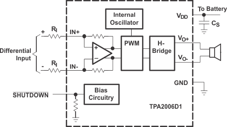
The TPA2006D1 device is a 1.45-W high efficiency filter-free class-D audio power amplifier in a 3 mm × 3 mm VSON package that requires only three external components. The SHUTDOWN pin is fully compatible with 1.8-V logic GPIO, such as are used on low-power cellular chipsets.
Features like 88% efficiency, –75-dB PSRR, improved RF-rectification immunity, and small total PCB footprint make the TPA2006D1 device ideal for cellular handsets. A fast start-up time of 1 ms with minimal pop makes the TPA2006D1 device ideal for PDA applications.
In cellular handsets, the earpiece, speaker phone, and melody ringer can each be driven by the TPA2006D1 device. The TPA2006D1 device allows independent gain while summing signals from separate sources, and has a low 36-μV noise floor, A-weighted.
The TPA2006D1 device has short-circuit and thermal protection.
Device Information(1)
| PART NUMBER | PACKAGE | BODY SIZE (NOM) |
|---|---|---|
| TPA2006D1 | VSON (8) | 3.00 mm ×3.00 mm |
- For all available packages, see the orderable addendum at the end of the datasheet.
Application Circuit
