SNAS279F April 2005 – July 2016 ADC084S021
PRODUCTION DATA.
- 1 Features
- 2 Applications
- 3 Description
- 4 Revision History
- 5 Device Comparison Table
- 6 Pin Configuration and Functions
- 7 Specifications
- 8 Detailed Description
- 9 Application and Implementation
- 10Power Supply Recommendations
- 11Layout
- 12Device and Documentation Support
- 13Mechanical, Packaging, and Orderable Information
Package Options
Mechanical Data (Package|Pins)
- DGS|10
Thermal pad, mechanical data (Package|Pins)
Orderable Information
11 Layout
11.1 Layout Guidelines
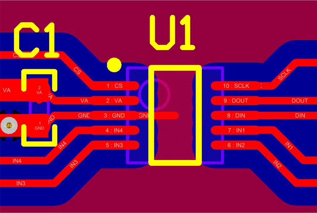
For optimum performance, take care with the physical layout of the ADC084S021 circuitry. The basic SAR architecture is sensitive to glitches or sudden changes on the power supply and ground connections that occur just prior to latching the output of the analog comparator. Therefore, during any single conversion for an n-bit SAR converter, there are n windows in which large external transient voltages can easily affect the conversion result. Such glitches might originate from switching power supplies, nearby digital logic, and high-power devices.
With this in mind, power to the ADC084S021 must be clean and well-bypassed. A 0.1-µF ceramic bypass capacitor must be placed as close to the device as possible. A 1-µF to 10-µF capacitor may also be needed if the impedance of the connection between VA and the power supply is high. Routing of the analog inputs must be kept short and separate from the digital lines. To keep unwanted coupling to a minimum, input traces must also be routed away from noisy components or planes that could crosstalk or interfere with the signal.
11.2 Layout Example
 Figure 51. ADC Layout