SBAS664B May 2014 – November 2014 ADC34J42 , ADC34J43 , ADC34J44 , ADC34J45
PRODUCTION DATA.
- 1 Features
- 2 Applications
- 3 Description
- 4 Revision History
- 5 Device Comparison Table
- 6 Pin Configuration and Functions
-
7 Specifications
- 7.1 Absolute Maximum Ratings
- 7.2 Handling Ratings
- 7.3 Recommended Operating Conditions
- 7.4 Summary of Special Mode Registers
- 7.5 Thermal Information
- 7.6 Electrical Characteristics: ADC34J44, ADC34J45
- 7.7 Electrical Characteristics: ADC34J42, ADC34J43
- 7.8 Electrical Characteristics: General
- 7.9 AC Performance: ADC34J45
- 7.10 AC Performance: ADC34J44
- 7.11 AC Performance: ADC34J43
- 7.12 AC Performance: ADC34J42
- 7.13 Digital Characteristics
- 7.14 Timing Characteristics
- 7.15 Typical Characteristics: ADC34J45
- 7.16 Typical Characteristics: ADC34J44
- 7.17 Typical Characteristics: ADC34J43
- 7.18 Typical Characteristics: ADC34J42
- 7.19 Typical Characteristics: Common Plots
- 7.20 Typical Characteristics: Contour Plots
- 8 Parameter Measurement Information
- 9 Detailed Description
- 10Application and Implementation
- 11Power-Supply Recommendations
- 12Layout
- 13Device and Documentation Support
- 14Mechanical, Packaging, and Orderable Information
Package Options
Mechanical Data (Package|Pins)
- RGZ|48
Thermal pad, mechanical data (Package|Pins)
- RGZ|48
Orderable Information
12 Layout
12.1 Layout Guidelines
The ADC34J4x EVM layout can be used as a reference layout to obtain the best performance. A layout diagram of the EVM top layer is provided in Figure 208. Some important points to remember while laying out the board are:
- Analog inputs are located on opposite sides of the device pin out to ensure minimum crosstalk on the package level. To minimize crosstalk onboard, the analog input traces exit the pin out in opposite directions, as shown in the reference layout of Figure 208 as much as possible.
- In the device pin out, the sampling clock is located on a side perpendicular to the analog inputs in order to minimize coupling between them. This configuration is also maintained on the reference layout of Figure 208 as much as possible.
- Keep digital outputs away from the analog inputs. When these digital outputs exit the pin out, do not keep the digital output traces parallel to the analog input traces because this configuration may result in coupling from digital outputs to analog inputs and degrade performance. Design all digital output traces to the receiver [such as a field-programmable gate array (FPGA) or an application-specific integrated circuit (ASIC)] to be matched in length to avoid skew among outputs.
- At each power-supply pin (AVDD and DVDD), keep a 0.1-µF decoupling capacitor close to the device. A separate decoupling capacitor group consisting of a parallel combination of 10-µF, 1-µF, and 0.1-µF capacitors can be kept close to the supply source.
12.2 Layout Example
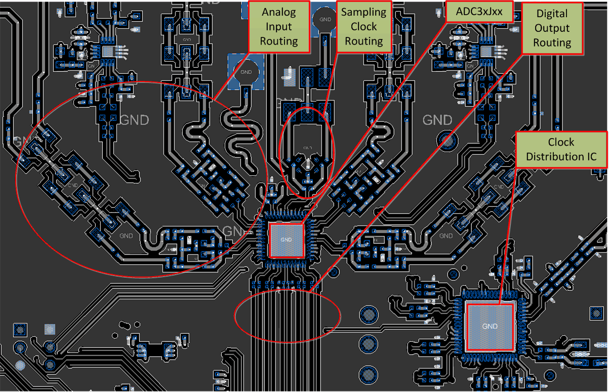 Figure 208. Typical Layout of the ADC34J4x Board