SBAS664B May 2014 – November 2014 ADC34J42 , ADC34J43 , ADC34J44 , ADC34J45
PRODUCTION DATA.
- 1 Features
- 2 Applications
- 3 Description
- 4 Revision History
- 5 Device Comparison Table
- 6 Pin Configuration and Functions
-
7 Specifications
- 7.1 Absolute Maximum Ratings
- 7.2 Handling Ratings
- 7.3 Recommended Operating Conditions
- 7.4 Summary of Special Mode Registers
- 7.5 Thermal Information
- 7.6 Electrical Characteristics: ADC34J44, ADC34J45
- 7.7 Electrical Characteristics: ADC34J42, ADC34J43
- 7.8 Electrical Characteristics: General
- 7.9 AC Performance: ADC34J45
- 7.10 AC Performance: ADC34J44
- 7.11 AC Performance: ADC34J43
- 7.12 AC Performance: ADC34J42
- 7.13 Digital Characteristics
- 7.14 Timing Characteristics
- 7.15 Typical Characteristics: ADC34J45
- 7.16 Typical Characteristics: ADC34J44
- 7.17 Typical Characteristics: ADC34J43
- 7.18 Typical Characteristics: ADC34J42
- 7.19 Typical Characteristics: Common Plots
- 7.20 Typical Characteristics: Contour Plots
- 8 Parameter Measurement Information
- 9 Detailed Description
- 10Application and Implementation
- 11Power-Supply Recommendations
- 12Layout
- 13Device and Documentation Support
- 14Mechanical, Packaging, and Orderable Information
Package Options
Mechanical Data (Package|Pins)
- RGZ|48
Thermal pad, mechanical data (Package|Pins)
- RGZ|48
Orderable Information
6 Pin Configuration and Functions
RGZ Package
VQFN-48
(Top View)
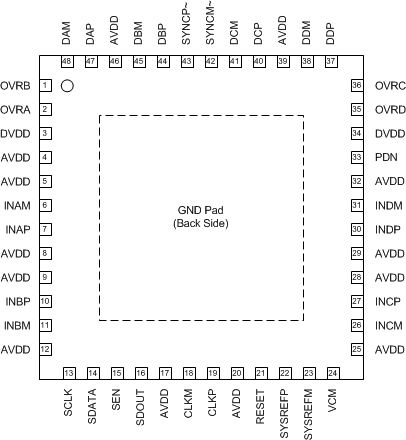
Pin Functions
| PIN | I/O | DESCRIPTION | |
|---|---|---|---|
| NAME | NO. | ||
| AVDD | 4, 5, 8, 9, 12, 17, 20, 25, 28, 29, 32, 39, 46 | I | Analog 1.8-V power supply |
| CLKM | 18 | I | Negative differential clock input for the ADC |
| CLKP | 19 | I | Positive differential clock input for the ADC |
| DAM | 48 | O | Negative serial JESD204B output for channel A |
| DAP | 47 | O | Positive serial JESD204B output for channel A |
| DBM | 45 | O | Negative serial JESD204B output for channel B |
| DBP | 44 | O | Positive serial JESD204B output for channel B |
| DCM | 41 | O | Negative serial JESD204B output for channel C |
| DCP | 40 | O | Positive serial JESD204B output for channel C |
| DDM | 38 | O | Negative serial JESD204B output for channel D |
| DDP | 37 | O | Positive serial JESD204B output for channel D |
| DVDD | 3, 34 | I | Digital 1.8-V power supply |
| GND | PowerPAD™ | I | Ground, 0 V |
| INAM | 6 | I | Negative differential analog input for channel A |
| INAP | 7 | I | Positive differential analog input for channel A |
| INBM | 11 | I | Negative differential analog input for channel B |
| INBP | 10 | I | Positive differential analog input for channel B |
| INCM | 26 | I | Negative differential analog input for channel C |
| INCP | 27 | I | Positive differential analog input for channel C |
| INDM | 31 | I | Negative differential analog input for channel D |
| INDP | 30 | I | Positive differential analog input for channel D |
| OVRA | 2 | O | Overrange indicator for channel A |
| OVRB | 1 | O | Overrange indicator for channel B |
| OVRC | 36 | O | Overrange indicator for channel C |
| OVRD | 35 | O | Overrange indicator for channel D |
| PDN | 33 | I | Power-down control. This pin has an internal 150-kΩ pull-down resistor. |
| RESET | 21 | I | Hardware reset; active high. This pin has an internal 150-kΩ, pull-down resistor. |
| SCLK | 13 | I | Serial interface clock input. This pin has an internal 150-kΩ pull-down resistor. |
| SDATA | 14 | I | Serial interface data input. This pin has an internal 150-kΩ pull-down resistor. |
| SDOUT | 16 | O | Serial interface data output |
| SEN | 15 | I | Serial interface enable. Active low. This pin has an internal 150-kΩ pull-up resistor to AVDD. |
| SYNCM~ | 42 | I | Negative JESD204B synch input |
| SYNCP~ | 43 | I | Positive JESD204B synch input |
| SYSREFM | 23 | I | Negative external SYSREF input |
| SYSREFP | 22 | I | Positive external SYSREF input |
| VCM | 24 | O | Common-mode voltage output for the analog inputs |