SBAS925A August   2018  – November 2018 ADS1119

PRODUCTION DATA.  

  1. Features
  2. Applications
  3. Description
    1.     Device Images
      1.      Voltage, Current, and Temperature Monitoring Application
  4. Revision History
  5. Pin Configuration and Functions
    1.     Pin Functions
  6. Specifications
    1. 6.1 Absolute Maximum Ratings
    2. 6.2 ESD Ratings
    3. 6.3 Recommended Operating Conditions
    4. 6.4 Thermal Information
    5. 6.5 Electrical Characteristics
    6. 6.6 I2C Timing Requirements
    7. 6.7 I2C Switching Characteristics
    8. 6.8 Typical Characteristics
  7. Parameter Measurement Information
    1. 7.1 Noise Performance
  8. Detailed Description
    1. 8.1 Overview
    2. 8.2 Functional Block Diagram
    3. 8.3 Feature Description
      1. 8.3.1 Multiplexer
      2. 8.3.2 Rail-to-Rail Input Buffers and Programmable Gain Stage
      3. 8.3.3 Voltage Reference
      4. 8.3.4 Modulator and Internal Oscillator
      5. 8.3.5 Digital Filter
      6. 8.3.6 Conversion Times
      7. 8.3.7 Offset Calibration
    4. 8.4 Device Functional Modes
      1. 8.4.1 Power-Up and Reset
        1. 8.4.1.1 Power-On Reset
        2. 8.4.1.2 RESET Pin
        3. 8.4.1.3 Reset by Command
      2. 8.4.2 Conversion Modes
        1. 8.4.2.1 Single-Shot Conversion Mode
        2. 8.4.2.2 Continuous Conversion Mode
      3. 8.4.3 Power-Down Mode
    5. 8.5 Programming
      1. 8.5.1 I2C Interface
        1. 8.5.1.1 I2C Address
        2. 8.5.1.2 Serial Clock (SCL) and Serial Data (SDA)
        3. 8.5.1.3 Data Ready (DRDY)
        4. 8.5.1.4 Interface Speed
        5. 8.5.1.5 Data Transfer Protocol
        6. 8.5.1.6 I2C General Call (Software Reset)
        7. 8.5.1.7 Timeout
      2. 8.5.2 Data Format
      3. 8.5.3 Commands
        1. 8.5.3.1 Command Latching
        2. 8.5.3.2 RESET (0000 011x)
        3. 8.5.3.3 START/SYNC (0000 100x)
        4. 8.5.3.4 POWERDOWN (0000 001x)
        5. 8.5.3.5 RDATA (0001 xxxx)
        6. 8.5.3.6 RREG (0010 0rxx)
        7. 8.5.3.7 WREG (0100 00xx dddd dddd)
      4. 8.5.4 Reading Data and Monitoring for New Conversion Results
    6. 8.6 Register Map
      1. 8.6.1 Configuration and Status Registers
      2. 8.6.2 Register Descriptions
        1. 8.6.2.1 Configuration Register (address = 0h) [reset = 00h]
          1. Table 10. Configuration Register Field Descriptions
        2. 8.6.2.2 Status Register (address = 1h) [reset = 00h]
          1. Table 11. Status Register Field Descriptions
  9. Application and Implementation
    1. 9.1 Application Information
      1. 9.1.1 Interface Connections
      2. 9.1.2 Connecting Multiple Devices on the Same I2C Bus
      3. 9.1.3 Unused Inputs and Outputs
      4. 9.1.4 Analog Input Filtering
      5. 9.1.5 External Reference and Ratiometric Measurements
      6. 9.1.6 Establishing Proper Limits on the Absolute Input Voltage
      7. 9.1.7 Pseudo Code Example
    2. 9.2 Typical Application
      1. 9.2.1 Design Requirements
      2. 9.2.2 Detailed Design Procedure
        1. 9.2.2.1 Voltage Monitoring
        2. 9.2.2.2 High-Side Current Measurement
        3. 9.2.2.3 Thermistor Measurement
        4. 9.2.2.4 Register Settings
      3. 9.2.3 Application Curve
  10. 10Power Supply Recommendations
    1. 10.1 Power-Supply Sequencing
    2. 10.2 Power-Supply Decoupling
  11. 11Layout
    1. 11.1 Layout Guidelines
    2. 11.2 Layout Example
  12. 12Device and Documentation Support
    1. 12.1 Device Support
      1. 12.1.1 Third-Party Products Disclaimer
    2. 12.2 Documentation Support
      1. 12.2.1 Related Documentation
    3. 12.3 Receiving Notification of Documentation Updates
    4. 12.4 Community Resources
    5. 12.5 Trademarks
    6. 12.6 Electrostatic Discharge Caution
    7. 12.7 Glossary
  13. 13Mechanical, Packaging, and Orderable Information

Package Options

Mechanical Data (Package|Pins)
Thermal pad, mechanical data (Package|Pins)
Orderable Information

Interface Connections

Figure 43 shows the principle interface connections for the ADS1119.
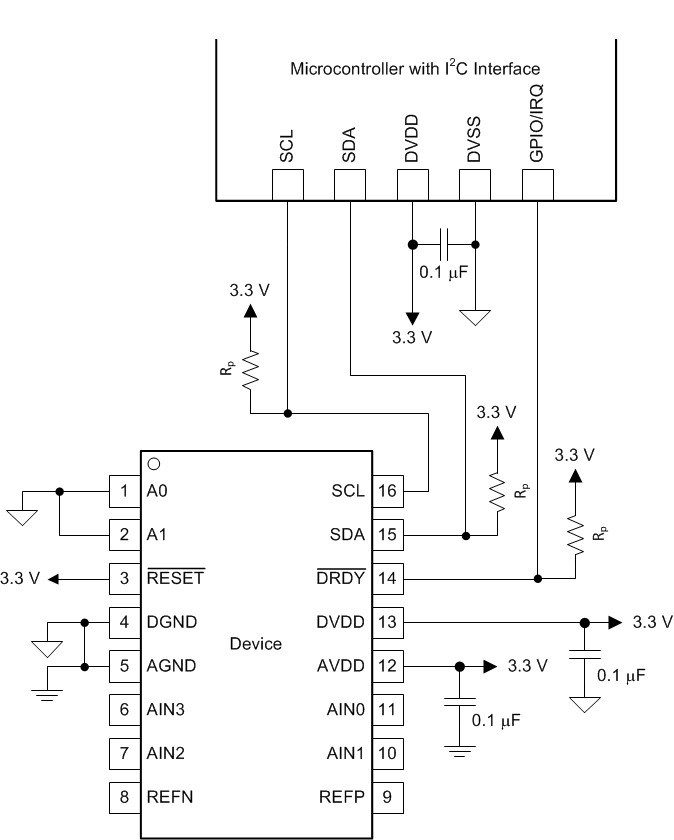
ADS1119 ai_mcu_connection_bas924.gifFigure 43. Interface Connections

The ADS1119 interfaces directly to standard-mode, fast-mode, or fast-mode plus I2C controllers. Any microcontroller I2C peripheral, including master-only and single-master I2C peripherals, operates with the ADS1119. Details of the I2C communication protocol of the device can be found in the Programming section. The ADS1119 does not perform clock-stretching (that is, the device never pulls the clock line low), so this function does not need to be provided for unless other clock-stretching devices are present on the same I2C bus.

Pullup resistors are required on both the SDA and SCL lines, as well as on the open-drain DRDY output. The size of these resistors depends on the bus operating speed and capacitance of the bus lines. Higher-value resistors yield lower power consumption when the bus lines are pulled low, but increase the transition times on the bus, which limits the bus speed. Lower-value resistors allow higher interface speeds, but at the expense of higher power consumption when the bus lines are pulled low. Long bus lines have higher capacitance and require smaller pullup resistors to compensate. Do not use resistors that are too small because the bus drivers may be unable to pull the bus lines low. See the I2C-Bus Specification and User Manual for details on pullup resistor sizing.