SBAS937B September 2018 – December 2018 ADS1278-SP
PRODUCTION DATA.
- 1 Features
- 2 Applications
- 3 Description
- 4 Revision History
- 5 Description (continued)
- 6 Pin Configuration and Functions
- 7 Specifications
-
8 Detailed Description
- 8.1 Overview
- 8.2 Functional Block Diagram
- 8.3
Feature Description
- 8.3.1 Sampling Aperture Matching
- 8.3.2 Frequency Response
- 8.3.3 Phase Response
- 8.3.4 Settling Time
- 8.3.5 Data Format
- 8.3.6 Analog Inputs (AINP, AINN)
- 8.3.7 Voltage Reference Inputs (VREFP, VREFN)
- 8.3.8 Clock Input (CLK)
- 8.3.9 Mode Selection (MODE)
- 8.3.10 Synchronization (SYNC)
- 8.3.11 Power-Down (PWDN)
- 8.3.12 Format[2:0]
- 8.3.13 Serial Interface Protocols
- 8.3.14 SPI Serial Interface
- 8.3.15 Frame-Sync Serial Interface
- 8.3.16 DOUT Modes
- 8.3.17 Daisy-Chaining
- 8.3.18 Modulator Output
- 8.3.19 Pin Test Using Test[1:0] Inputs
- 8.3.20 VCOM Output
- 8.4 Device Functional Modes
- 9 Application and Implementation
- 10Power Supply Recommendations
- 11Layout
- 12Device and Documentation Support
- 13Mechanical, Packaging, and Orderable Information
Package Options
Mechanical Data (Package|Pins)
- HFQ|84
Thermal pad, mechanical data (Package|Pins)
Orderable Information
8.3.2.2 High-Resolution Mode
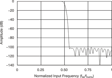
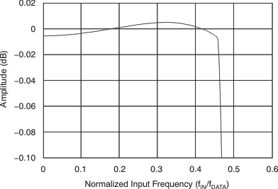
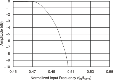
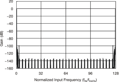
The oversampling ratio is 128 in High-Resolution mode. Figure 58 shows the frequency response in High-Resolution mode normalized to fDATA. Figure 59 shows the passband ripple, and the transition from passband to stop band is shown in Figure 60. The overall frequency response repeats at multiples of the modulator frequency fMOD (128 × fDATA), as shown in Figure 61. The stop band of the ADS1278-SP provides 100-dB attenuation of frequencies that begin just beyond the passband and continue out to fMOD. Placing an antialiasing, low-pass filter in front of the ADS1278-SP inputs is recommended to limit possible high-amplitude out-of-band signals and noise. Often, a simple RC filter is sufficient. Table 2 lists the image rejection versus external filter order.
 Figure 58. Frequency Response For High-Resolution Mode
  Figure 59. Passband Response For High-Resolution Mode
  Figure 60. Transition Band Response For High-Resolution Mode
  Figure 61. Frequency Response Out To FMOD For High-Resolution Mode