SBAS937B September 2018 – December 2018 ADS1278-SP
PRODUCTION DATA.
- 1 Features
- 2 Applications
- 3 Description
- 4 Revision History
- 5 Description (continued)
- 6 Pin Configuration and Functions
- 7 Specifications
-
8 Detailed Description
- 8.1 Overview
- 8.2 Functional Block Diagram
- 8.3
Feature Description
- 8.3.1 Sampling Aperture Matching
- 8.3.2 Frequency Response
- 8.3.3 Phase Response
- 8.3.4 Settling Time
- 8.3.5 Data Format
- 8.3.6 Analog Inputs (AINP, AINN)
- 8.3.7 Voltage Reference Inputs (VREFP, VREFN)
- 8.3.8 Clock Input (CLK)
- 8.3.9 Mode Selection (MODE)
- 8.3.10 Synchronization (SYNC)
- 8.3.11 Power-Down (PWDN)
- 8.3.12 Format[2:0]
- 8.3.13 Serial Interface Protocols
- 8.3.14 SPI Serial Interface
- 8.3.15 Frame-Sync Serial Interface
- 8.3.16 DOUT Modes
- 8.3.17 Daisy-Chaining
- 8.3.18 Modulator Output
- 8.3.19 Pin Test Using Test[1:0] Inputs
- 8.3.20 VCOM Output
- 8.4 Device Functional Modes
- 9 Application and Implementation
- 10Power Supply Recommendations
- 11Layout
- 12Device and Documentation Support
- 13Mechanical, Packaging, and Orderable Information
Package Options
Mechanical Data (Package|Pins)
- HFQ|84
Thermal pad, mechanical data (Package|Pins)
Orderable Information
8.3.9 Mode Selection (MODE)
The ADS1278-SP supports four modes of operation: High-Speed, High-Resolution, Low-Power, and Low-Speed. The modes offer optimization of speed, resolution, and power. Mode selection is determined by the status of the digital input MODE[1:0] pins, as shown in Table 6. The ADS1278-SP continually monitors the status of the MODE pin during operation.
Table 6. Mode Selection
| MODE[1:0] | MODE SELECTION | MAX fDATA(1) |
|---|---|---|
| 00 | High-Speed | 128,000 |
| 01 | High-Resolution | 52,734 |
| 10 | Low-Power | 52,734 |
| 11 | Low-Speed | 10,547 |
| (1) fCLK = 27-MHz max (32.768-MHz max in High-Speed mode). |
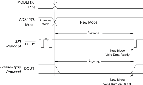
When using the SPI protocol, DRDY is held high after a mode change occurs until settled (or valid) data are ready; see Figure 68 and Table 7.
In Frame-Sync protocol, the DOUT pins are held low after a mode change occurs until settled data are ready; see Figure 68 and Table 7. Data can be read from the device to detect when DOUT changes to logic 1, indicating that the data are valid.
 Figure 68. Mode Change Timing
 Table 7. New Data After Mode Change
| SYMBOL | DESCRIPTION | MIN | TYP | MAX | UNITS |
|---|---|---|---|---|---|
| tNDR-SPI | Time for new data to be ready (SPI) | 129 | Conversions (1/fDATA) | ||
| tNDR-FS | Time for new data to be ready (Frame-Sync) | 127 | 128 | Conversions (1/fDATA) |