SBAS853A January 2020 – April 2021 ADS131M02
PRODUCTION DATA
- 1 Features
- 2 Applications
- 3 Description
- 4 Revision History
- 5 Pin Configuration and Functions
- 6 Specifications
- 7 Parameter Measurement Information
-
8 Detailed Description
- 8.1 Overview
- 8.2 Functional Block Diagram
- 8.3
Feature Description
- 8.3.1 Input ESD Protection Circuitry
- 8.3.2 Input Multiplexer
- 8.3.3 Programmable Gain Amplifier (PGA)
- 8.3.4 Voltage Reference
- 8.3.5 Clocking and Power Modes
- 8.3.6 ΔΣ Modulator
- 8.3.7 Digital Filter
- 8.3.8 DC Block Filter
- 8.3.9 Internal Test Signals
- 8.3.10 Channel Phase Calibration
- 8.3.11 Calibration Registers
- 8.3.12 Communication Cyclic Redundancy Check (CRC)
- 8.3.13 Register Map CRC
- 8.4 Device Functional Modes
- 8.5
Programming
- 8.5.1
Interface
- 8.5.1.1 Chip Select (CS)
- 8.5.1.2 Serial Data Clock (SCLK)
- 8.5.1.3 Serial Data Input (DIN)
- 8.5.1.4 Serial Data Output (DOUT)
- 8.5.1.5 Data Ready (DRDY)
- 8.5.1.6 Conversion Synchronization or System Reset (SYNC/RESET)
- 8.5.1.7 SPI Communication Frames
- 8.5.1.8 SPI Communication Words
- 8.5.1.9 ADC Conversion Data
- 8.5.1.10
Commands
- 8.5.1.10.1 NULL (0000 0000 0000 0000)
- 8.5.1.10.2 RESET (0000 0000 0001 0001)
- 8.5.1.10.3 STANDBY (0000 0000 0010 0010)
- 8.5.1.10.4 WAKEUP (0000 0000 0011 0011)
- 8.5.1.10.5 LOCK (0000 0101 0101 0101)
- 8.5.1.10.6 UNLOCK (0000 0110 0110 0110)
- 8.5.1.10.7 RREG (101a aaaa annn nnnn)
- 8.5.1.10.8 WREG (011a aaaa annn nnnn)
- 8.5.1.11 Short SPI Frames
- 8.5.2 Synchronization
- 8.5.1
Interface
- 8.6 ADS131M02 Registers
- 9 Application and Implementation
- 10Power Supply Recommendations
- 11Layout
- 12Device and Documentation Support
- 13Mechanical, Packaging, and Orderable Information
Package Options
Mechanical Data (Package|Pins)
Thermal pad, mechanical data (Package|Pins)
- RUK|20
Orderable Information
9.1.2 Antialiasing
An analog low-pass filter is required in front of each of the channel inputs to prevent out-of-band noise and interferers from coupling into the band of interest. Because the ADS131M02 is a delta-sigma ADC, the integrated digital filter provides substantial attenuation for frequencies outside of the band of interest up to the frequencies adjacent to fMOD. Therefore, a single-order RC filter provides sufficient antialiasing protection in the vast majority of applications.
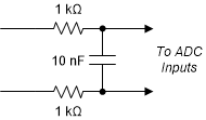
Choosing the values of the resistor and capacitor depends on the desired cutoff frequency, limiting source impedance for the ADC inputs, and providing enough instantaneous charge to the ADC input sampling circuit through the filter capacitor. Figure 9-1 shows the recommended filter component values. These recommendations are sufficient for CLKIN frequencies between 2 MHz and 8.2 MHz.
 Figure 9-1 Recommended Antialiasing Circuitry