SBAS889A January 2020 – April 2021 ADS131M03
PRODUCTION DATA
- 1 Features
- 2 Applications
- 3 Description
- 4 Revision History
- 5 Pin Configuration and Functions
- 6 Specifications
- 7 Parameter Measurement Information
-
8 Detailed Description
- 8.1 Overview
- 8.2 Functional Block Diagram
- 8.3
Feature Description
- 8.3.1 Input ESD Protection Circuitry
- 8.3.2 Input Multiplexer
- 8.3.3 Programmable Gain Amplifier (PGA)
- 8.3.4 Voltage Reference
- 8.3.5 Clocking and Power Modes
- 8.3.6 ΔΣ Modulator
- 8.3.7 Digital Filter
- 8.3.8 DC Block Filter
- 8.3.9 Internal Test Signals
- 8.3.10 Channel Phase Calibration
- 8.3.11 Calibration Registers
- 8.3.12 Communication Cyclic Redundancy Check (CRC)
- 8.3.13 Register Map CRC
- 8.4 Device Functional Modes
- 8.5
Programming
- 8.5.1
Interface
- 8.5.1.1 Chip Select (CS)
- 8.5.1.2 Serial Data Clock (SCLK)
- 8.5.1.3 Serial Data Input (DIN)
- 8.5.1.4 Serial Data Output (DOUT)
- 8.5.1.5 Data Ready (DRDY)
- 8.5.1.6 Conversion Synchronization or System Reset (SYNC/RESET)
- 8.5.1.7 SPI Communication Frames
- 8.5.1.8 SPI Communication Words
- 8.5.1.9 ADC Conversion Data
- 8.5.1.10
Commands
- 8.5.1.10.1 NULL (0000 0000 0000 0000)
- 8.5.1.10.2 RESET (0000 0000 0001 0001)
- 8.5.1.10.3 STANDBY (0000 0000 0010 0010)
- 8.5.1.10.4 WAKEUP (0000 0000 0011 0011)
- 8.5.1.10.5 LOCK (0000 0101 0101 0101)
- 8.5.1.10.6 UNLOCK (0000 0110 0110 0110)
- 8.5.1.10.7 RREG (101a aaaa annn nnnn)
- 8.5.1.10.8 WREG (011a aaaa annn nnnn)
- 8.5.1.11 Short SPI Frames
- 8.5.2 Synchronization
- 8.5.1
Interface
- 8.6 ADS131M03 Registers
- 9 Application and Implementation
- 10Power Supply Recommendations
- 11Layout
- 12Device and Documentation Support
- 13Mechanical, Packaging, and Orderable Information
Package Options
Mechanical Data (Package|Pins)
Thermal pad, mechanical data (Package|Pins)
- RUK|20
Orderable Information
8.5.1.9.1 Collecting Data for the First Time or After a Pause in Data Collection
Take special precaution when collecting data for the first time or when beginning to collect data again after a pause. The internal mechanism that outputs data contains a first-in-first-out (FIFO) buffer that can store two samples of data per channel at a time. The DRDY flag for each channel in the STATUS register remains set until both samples for each channel are read from the device. This condition is not obvious under normal circumstances when the host is reading each consecutive sample from the device. In that case, the samples are cleared from the device each time new data are generated so the DRDY flag for each channel in the STATUS register is cleared with each read. However, both slots of the FIFO are full if a sample is missed or if data are not read for a period of time. Either strobe the SYNC/RESET pin to re-synchronize conversions and clear the FIFOs, or quickly read two data packets when data are read for the first time or after a gap in reading data. This process ensures predictable DRDY pin behavior. See the Section 8.5.2 section for information about the synchronization feature. These methods do not need to be employed if each channel data was read for each output data period from when the ADC was enabled.
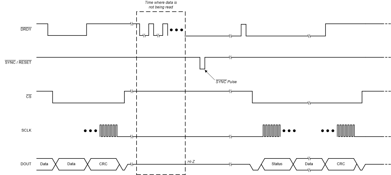
Figure 8-20 depicts an example of how to collect data after a period of the ADC running, but where no data are being retrieved. In this instance, the SYNC/RESET pin is used to clear the internal FIFOs and realign the ADS131M03 output data with the host.
 Figure 8-20 Collecting Data After a Pause in Data
Collection Using the SYNC/RESET
Pin
Figure 8-20 Collecting Data After a Pause in Data
Collection Using the SYNC/RESET
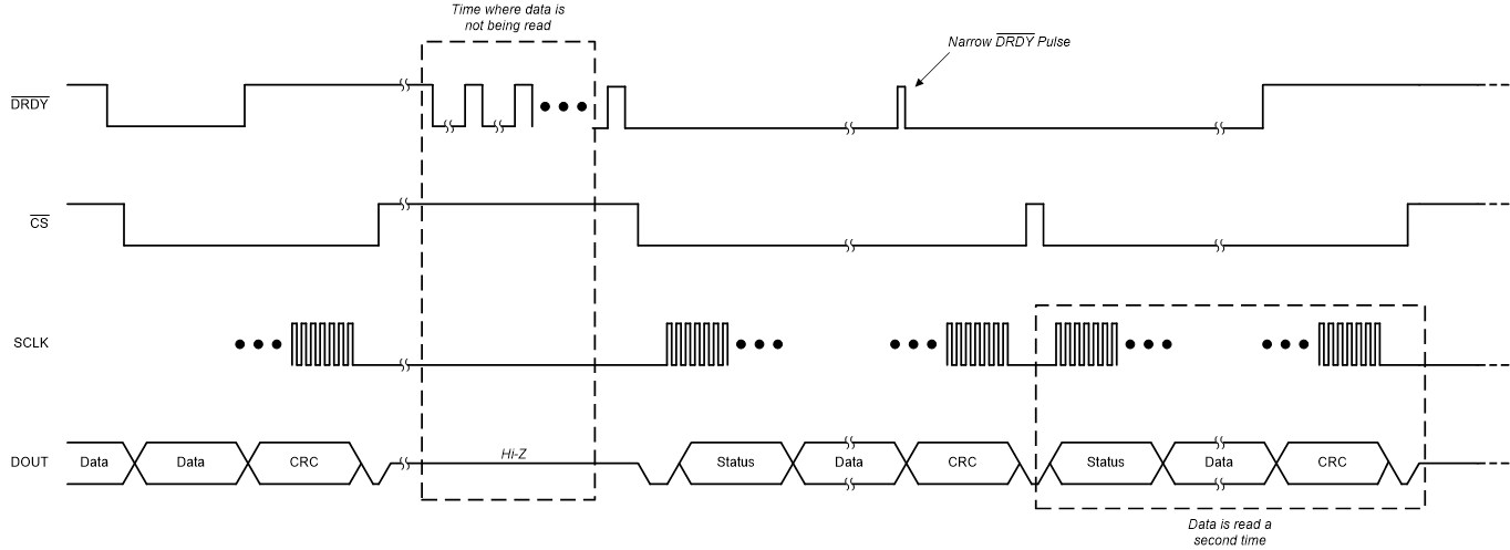
PinAnother functionally equivalent method for clearing the FIFO after a pause in collecting data is to begin by reading two samples in quick succession. Figure 8-21 depicts this method. This example shows when the DRDY_FMT bit in the MODE register is set to 0b indicating DRDY is a level output. There is a very narrow pulse on DRDY immediately after the first set of data are shifted out of the device. This pulse may be too narrow for some microcontrollers to detect. Therefore, do not rely upon this pulse but instead immediately read out the second data set after the first data set. The host operates synchronous to the device after the second word is read from the device.
 Figure 8-21 Collecting Data After a Pause in Data
Collection by Reading Data Twice