SBAS653B April 2014 – October 2020 ADS4245-EP
PRODUCTION DATA
- 1 Features
- 2 Applications
- 3 Description
- 4 Revision History
- 5 Pin Configuration and Functions
-
6 Specifications
- 6.1 Absolute Maximum Ratings
- 6.2 ESD Ratings
- 6.3 Recommended Operating Conditions
- 6.4 Thermal Information
- 6.5 Electrical Characteristics:
- 6.6 Electrical Characteristics: General
- 6.7 Digital Characteristics
- 6.8 Timing Characteristics: LVDS And CMOS Modes
- 6.9 Typical Characteristics:
- 6.10 Typical Characteristics: General
- 6.11 Typical Characteristics: Contour
-
7 Detailed Description
- 7.1 Overview
- 7.2 Functional Block Diagram
- 7.3 Feature Description
- 7.4 Device Functional Modes
- 7.5 Serial Register Map
- 7.6 Description Of Serial Registers
- 8 Application Information Disclaimer
- 9 Power Supply Recommendations
- 10Layout
- 11Device and Documentation Support
- 12Mechanical, Packaging, and Orderable Information
Package Options
Mechanical Data (Package|Pins)
- RGC|64
Thermal pad, mechanical data (Package|Pins)
- RGC|64
Orderable Information
6.8 Timing Characteristics: LVDS And CMOS Modes
Typical values are at +25°C, AVDD = 1.8 V, DRVDD = 1.8V, sampling frequency =
160MSPS, sine wave input clock, 1.5VPP clock amplitude,
CLOAD = 5pF(2), and RLOAD = 100Ω(3), unless otherwise noted. Minimum and maximum values are across the full
temperature range: TMIN = –55°C to TMAX = +125°C, AVDD =
1.8V, and DRVDD = 1.7V to 1.9V.
| PARAMETER(1) | DESCRIPTION | MIN | TYP | MAX | UNIT | |
|---|---|---|---|---|---|---|
| tA | Aperture delay | 0.8 | ns | |||
| Aperture delay matching | Between the two channels of the same device | ±70 | ps | |||
| Variation of aperture delay | Between two devices at the same temperature and DRVDD supply | ±150 | ps | |||
| tJ | Aperture jitter | 140 | fS rms | |||
| Wakeup time | Time to valid data after coming out of STANDBY mode | 50 | 100 | µs | ||
| Time to valid data after coming out of GLOBAL power-down mode | 100 | 500 | µs | |||
| ADC latency(7) | Default latency after reset | 16 | Clock cycles | |||
| Digital functions enabled (EN DIGITAL = 1) | 24 | Clock cycles | ||||
| DDR LVDS MODE(4) | ||||||
| tSU | Data setup time | Data valid(5) to zero-crossing of CLKOUTP | 1.5 | 2.0 | ns | |
| tH | Data hold time | Zero-crossing of CLKOUTP to data becoming invalid(5) | 0.35 | 0.6 | ns | |
| tPDI | Clock propagation delay | Input clock rising edge cross-over to output clock rising edge cross-over | 5.0 | 6.1 | 7.5 | ns |
| LVDS bit clock duty cycle | Duty cycle of differential clock, (CLKOUTP-CLKOUTM) | 49 | % | |||
| tRISE, tFALL |
Data rise time, Data fall time |
Rise time measured from –100mV to +100mV Fall time measured from +100mV to –100mV 1MSPS ≤ Sampling frequency ≤ 160MSPS |
0.13 | ns | ||
| tCLKRISE, tCLKFALL |
Output clock rise time, Output clock fall time |
Rise time measured from –100mV to +100mV Fall time measured from +100mV to –100mV 1MSPS ≤ Sampling frequency ≤ 160MSPS |
0.13 | ns | ||
| PARALLEL CMOS MODE | ||||||
| tSU | Data setup time | Data valid(6) to zero-crossing of CLKOUT | 1.6 | 2.5 | ns | |
| tH | Data hold time | Zero-crossing of CLKOUT to data becoming invalid(6) | 2.3 | 2.7 | ns | |
| tPDI | Clock propagation delay | Input clock rising edge cross-over to output clock rising edge cross-over | 4.5 | 6.4 | 8.5 | ns |
| Output clock duty cycle | Duty cycle of output clock, CLKOUT 1MSPS ≤ Sampling frequency ≤ 160MSPS |
46 | % | |||
| tRISE, tFALL |
Data rise time, Data fall time |
Rise time measured from 20% to 80% of DRVDD Fall time measured from 80% to 20% of DRVDD 1MSPS ≤ Sampling frequency ≤ 160MSPS |
1 | ns | ||
| tCLKRISE, tCLKFALL |
Output clock rise time Output clock fall time |
Rise time measured from 20% to 80% of DRVDD Fall time measured from 80% to 20% of DRVDD 1MSPS ≤ Sampling frequency ≤ 160MSPS |
1 | ns | ||
(1) Timing parameters are ensured by design and characterization and not tested in
production.
(2) CLOAD is the effective external single-ended load capacitance between
each output terminal and ground
(3) RLOAD is the differential load resistance between the LVDS output
pair.
(4) Measurements are done with a transmission line of 100 Ω characteristic impedance
between the device and the load. Setup and hold time specifications take into
account the effect of jitter on the output data and clock.
(5) Data valid refers to a logic high
of +100 mV and a logic low of –100 mV.
(6) Data valid refers to a logic high
of 1.26 V and a logic low of 0.54 V
(7) At higher frequencies, tPDI is greater than one clock period and
overall latency = ADC latency + 1.
Table 6-2 LVDS Timings At Lower Sampling Frequencies
| SAMPLING FREQUENCY (MSPS) | SETUP TIME (ns) | HOLD TIME (ns) | tPDI, CLOCK PROPAGATION DELAY (ns) |
||||||
|---|---|---|---|---|---|---|---|---|---|
| MIN | TYP | MAX | MIN | TYP | MAX | MIN | TYP | MAX | |
| 65 | 5.9 | 6.6 | 0.35 | 0.6 | 5.0 | 6.1 | 7.5 | ||
| 80 | 4.5 | 5.2 | 0.35 | 0.6 | 5.0 | 6.1 | 7.5 | ||
| 125 | 2.3 | 2.9 | 0.35 | 0.6 | 5.0 | 6.1 | 7.5 | ||
Table 6-3 CMOS Timings At Lower Sampling Frequencies
| SAMPLING FREQUENCY (MSPS) | TIMINGS SPECIFIED WITH RESPECT TO CLKOUT | ||||||||
|---|---|---|---|---|---|---|---|---|---|
| SETUP TIME (ns) | HOLD TIME (ns) | tPDI, CLOCK PROPAGATION DELAY (ns) |
|||||||
| MIN | TYP | MAX | MIN | TYP | MAX | MIN | TYP | MAX | |
| 65 | 6.1 | 7.2 | 6.7 | 7.1 | 4.5 | 6.4 | 8.5 | ||
| 80 | 4.7 | 5.8 | 5.3 | 5.8 | 4.5 | 6.4 | 8.5 | ||
| 125 | 2.7 | 3.6 | 3.1 | 3.6 | 4.5 | 6.4 | 8.5 | ||

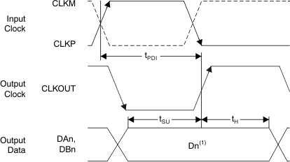
A. Dn = bits D0, D1, D2,
etc. of channels A and B.
Figure 6-3 CMOS Interface Timing Diagram
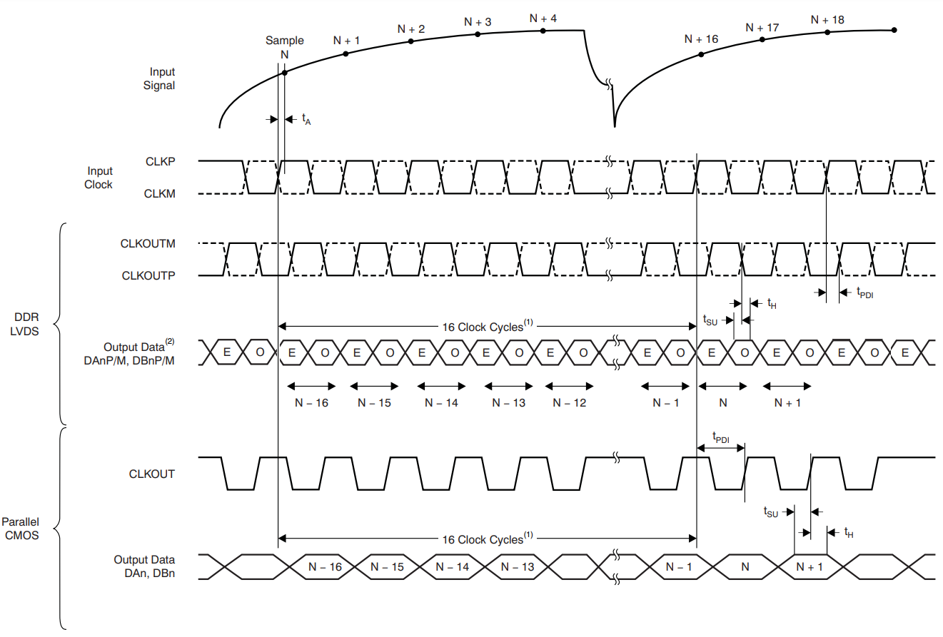
A. ADC latency after reset.
At higher sampling frequencies, tPDI is greater than one clock cycle,
which then makes the overall latency = ADC latency + 1.
B. E = even bits (D0, D2, D4, etc.); O = odd
bits (D1, D3, D5, etc.).
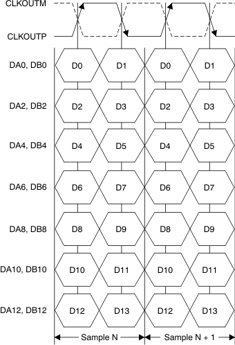
Figure 6-4 Latency Timing Diagram Figure 6-5 ADS4245 LVDS Interface Timing Diagram