SLWS207B May 2008 – January 2016 ADS5560 , ADS5562
PRODUCTION DATA.
- 1 Features
- 2 Applications
- 3 Description
- 4 Revision History
- 5 Pin Configuration and Functions
-
6 Specifications
- 6.1 Absolute Maximum Ratings
- 6.2 ESD Ratings
- 6.3 Recommended Operating Conditions
- 6.4 Thermal Information
- 6.5 Electrical Characteristics
- 6.6 AC Electrical Characteristics for ADS5560 Fs = 40 MSPS
- 6.7 AC Electrical Characteristics for ADS5562, Fs = 80 MSPS
- 6.8 Electrical Characteristics for ADS5562
- 6.9 Electrical Characteristics for ADS5560
- 6.10 Digital Characteristics
- 6.11 Timing Characteristics for LVDS and CMOS Modes
- 6.12 Serial Interface Timing Characteristics
- 6.13 Reset Timing
- 6.14 Timing Characteristics at Lower Sampling Frequencies
- 6.15 Typical Characteristics
- 7 Detailed Description
- 8 Application and Implementation
- 9 Power Supply Recommendations
- 10Layout
- 11Device and Documentation Support
- 12Mechanical, Packaging, and Orderable Information
Package Options
Mechanical Data (Package|Pins)
- RGZ|48
Thermal pad, mechanical data (Package|Pins)
- RGZ|48
Orderable Information
1 Features
- 16-Bit Resolution
- Maximum Sample Rate:
- ADS5562: 80 MSPS
- ADS5560: 40 MSPS
- Total Power:
- 865 mW at 80 MSPS
- 674 mW at 40 MSPS
- No Missing Codes
- High SNR: 84 dBFS (3 MHz IF)
- SFDR: 85 dBc (3 MHz IF)
- Low-Frequency Noise Suppression Mode
- Programmable Fine Gain, 1-dB steps Until 6-dB Maximum Gain
- Double Data-Rate (DDR) LVDS and Parallel CMOS Output Options
- Internal and External Reference Support
- 3.3-V Analog and Digital Supply
- Pin-for-Pin With ADS5547 Family
- 48-VQFN Package (7.00 mm × 7.00 mm)
2 Applications
- Medical Imaging, MRI
- Wireless Communications Infrastructure
- Software Defined Radio
- Test and Measurement Instrumentation
- High Definition Video
3 Description
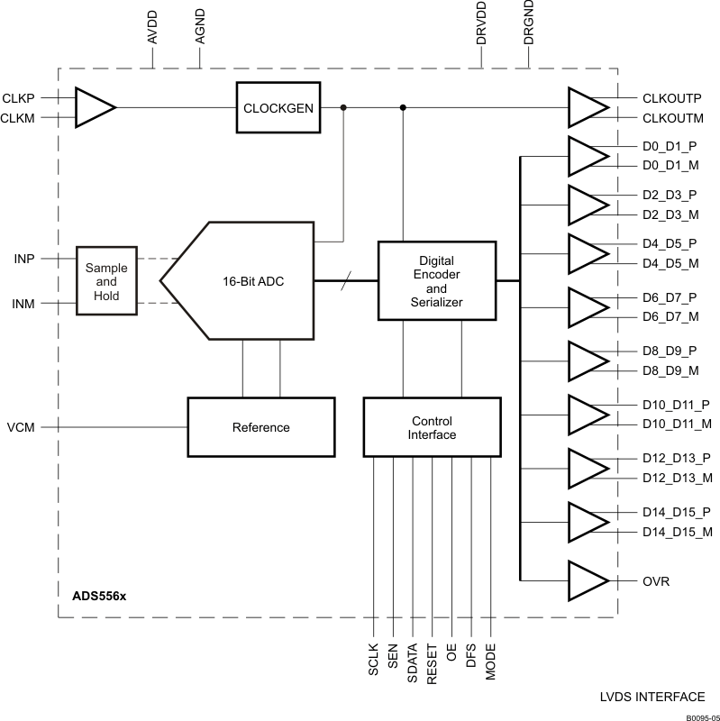
The ADS556x is a high-performance 16-bit family of ADCs with sampling rates up to 80 MSPS. The device supports very-high SNR for input frequencies in the first Nyquist zone. The device includes a low-frequency noise suppression mode that improves the noise from DC to about 1 MHz.
In addition to high performance, the device offers several flexible features such as output interface (either Double Data Rate [DDR] LVDS or parallel CMOS) and fine gain in 1-dB steps until 6-dB maximum gain.
Innovative techniques, such as DDR LVDS and an internal reference that does not require external decoupling capacitors, have been used to achieve significant savings in pin count. This innovation results in a compact 7-mm × 7-mm 48-pin VQFN package.
The device can be put in an external reference mode, where the VCM pin behaves as the external reference input. For applications where power is important, the ADS556x device offers power down modes and automatic power scaling at lower sample rates.
The device is specified over the industrial temperature range of –40°C to 85°C.
Device Information(1)
| PART NUMBER | PACKAGE | BODY SIZE (NOM) |
|---|---|---|
| ADS5560 | VQFN (48) | 7.00 mm × 7.00 mm |
| ADS5562 |
- For all available packages, see the orderable addendum at the end of the data sheet.
Block Diagram

4 Revision History
Changes from A Revision (May 2012) to B Revision
- Added ESD Ratings table, Feature Description section, Device Functional Modes, Application and Implementation section, Power Supply Recommendations section, Layout section, Device and Documentation Support section, and Mechanical, Packaging, and Orderable Information section.Go
Changes from * Revision (May 2008) to A Revision
- Changed Programmable Fine Gain in FEATURESGo
- Added maximum gain to end of second paragraph of DESCRIPTIONGo
- Changed Voltage between AVDD to DRVDD to Voltage between AVDD and DRVDD in ABS MAX RATINGSGo
- Added Voltage applied to analog input pins, INP, INM in ABS MAX RATINGSGo
- Added Voltage applied to analog input pins, CLKP, CLKM, MODE in ABS MAX RATINGSGo
- Added Voltage applied to analog input pins, RESET, SCLK, SDATA, SEN, OE, DFS in ABS MAX RATINGSGo
- Changed boundary between DEFAULT SPEED mode and LOW SPEED mode from 30 MSPS to 25 MSPS in RECOMMENDED OPERATING CONDITIONS Go
- Changed tho to th in header row of Timing Characteristics at Lower Sampling FrequenciesGo
- Added text to Note regarding RESET pulse requirement in Figure 1Go
- Added 32k Point FFT to TYPICAL CHARACTERISTICS section conditions Go
- Changed Figure 48Go
- Added text to end of Programmable Fine Gain sectionGo
- Added (Serial Interface Mode) to Table 1 titleGo
- Changed LOW SPEED mode boundary from 30 MSPS to 25 MSPS in Low Sampling Frequency Operation sectionGo
- Added text to Clock Input sectionGo
- Changed Clock Input section paragraphs and 4 illustrationsGo
- Added (of width greater than 10ns) in USING SERIAL INTERFACE PROGRAMMING ONLY sectionGo
- Added to Priority last row in Table 3 Go
- Changed Parallel Interface Control description for SCLK Control Pin, (SCLK = 0, 3dB gain; SCLK = DRVDD, 1 dB gain) in Table 4Go
- Changed first pargraph in SERIAL INTERFACE sectionGo
- Added text to Table 9 NoteGo
- Changed Fs > 30 MSPS to Fs > 25 MSPS in <LOW SPEED> Go