SBAS652A May 2014 – August 2014 ADS7950-Q1 , ADS7951-Q1 , ADS7952-Q1 , ADS7953-Q1 , ADS7954-Q1 , ADS7956-Q1 , ADS7957-Q1 , ADS7958-Q1 , ADS7959-Q1 , ADS7960-Q1 , ADS7961-Q1
PRODUCTION DATA.
- 1 Features
- 2 Applications
- 3 Description
- 4 Revision History
- 5 Device Comparison Table
- 6 Pin Configurations and Functions
-
7 Specifications
- 7.1 Absolute Maximum Ratings
- 7.2 Handling Ratings
- 7.3 Recommended Operating Conditions
- 7.4 Thermal Information
- 7.5 Electrical Characteristics: ADS7950-Q1, ADS7951-Q1, ADS7952-Q1, ADS7953-Q1
- 7.6 Electrical Characteristics: ADS7954-Q1, ADS7956-Q1, ADS7957-Q1
- 7.7 Electrical Characteristics: ADS7958-Q1, ADS7959-Q1, ADS7960-Q1, ADS7961-Q1
- 7.8 Timing Requirements
- 7.9 Typical Characteristics (All ADS79xx-Q1 Family Devices)
- 7.10 Typical Characteristics (12-Bit Devices Only)
- 8 Detailed Description
- 9 Application and Implementation
- 10Power-Supply Recommendations
- 11Layout
- 12Device and Documentation Support
- 13Mechanical, Packaging, and Orderable Information
Package Options
Mechanical Data (Package|Pins)
- DBT|30
Thermal pad, mechanical data (Package|Pins)
Orderable Information
11 Layout
11.1 Layout Guidelines
- A copper fill area underneath the device ties the AGND, BDGND, AINM, and REFM pins together. This copper fill area must also be connected to the analog ground plane of the PCB using at least four vias.
- The power sources must be clean and properly decoupled by placing a capacitor close to each of the three supply pins, as shown in Figure 64. To minimize ground inductance, ensure that each capacitor ground pin is connected to a grounding via by a very short and thick trace.
- The REFP pin requires a 10-μF ceramic capacitor to meet performance specifications. Place the capacitor directly next to the device. This capacitor ground pin must be routed to the REFM pin by a very short trace, as shown in Figure 64.
- Do not place any vias between a capacitor pin and a device pin.
NOTE
The full-power bandwidth of the converter makes the ADC sensitive to high frequencies in digital lines. Organize components in the PCB by keeping digital lines apart from the analog signal paths. This design configuration is critical to minimize crosstalk. For example, in Figure 64, input drivers are expected to be on the left of the converter and the microcontroller on the right.
11.2 Layout Example
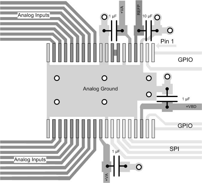 Figure 64. Layout Example