SBAS652A May 2014 – August 2014 ADS7950-Q1 , ADS7951-Q1 , ADS7952-Q1 , ADS7953-Q1 , ADS7954-Q1 , ADS7956-Q1 , ADS7957-Q1 , ADS7958-Q1 , ADS7959-Q1 , ADS7960-Q1 , ADS7961-Q1
PRODUCTION DATA.
- 1 Features
- 2 Applications
- 3 Description
- 4 Revision History
- 5 Device Comparison Table
- 6 Pin Configurations and Functions
-
7 Specifications
- 7.1 Absolute Maximum Ratings
- 7.2 Handling Ratings
- 7.3 Recommended Operating Conditions
- 7.4 Thermal Information
- 7.5 Electrical Characteristics: ADS7950-Q1, ADS7951-Q1, ADS7952-Q1, ADS7953-Q1
- 7.6 Electrical Characteristics: ADS7954-Q1, ADS7956-Q1, ADS7957-Q1
- 7.7 Electrical Characteristics: ADS7958-Q1, ADS7959-Q1, ADS7960-Q1, ADS7961-Q1
- 7.8 Timing Requirements
- 7.9 Typical Characteristics (All ADS79xx-Q1 Family Devices)
- 7.10 Typical Characteristics (12-Bit Devices Only)
- 8 Detailed Description
- 9 Application and Implementation
- 10Power-Supply Recommendations
- 11Layout
- 12Device and Documentation Support
- 13Mechanical, Packaging, and Orderable Information
Package Options
Mechanical Data (Package|Pins)
- DBT|30
Thermal pad, mechanical data (Package|Pins)
Orderable Information
6 Pin Configurations and Functions
DBT Package
TSSOP-30
(Top View)
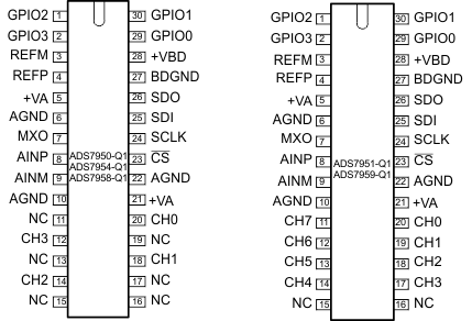
NC = No internal connection
DBT Package
TSSOP-38
(Top View)
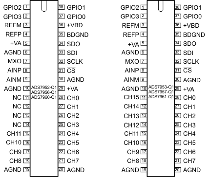
Pin Functions
| PIN | I/O | DESCRIPTION | |||||
|---|---|---|---|---|---|---|---|
| NAME | NUMBER | ||||||
| ADS7953-Q1, ADS7957-Q1, ADS7961-Q1 |
ADS7952-Q1, ADS7956-Q1, ADS7960-Q1 |
ADS7951-Q1, ADS7959-Q1 |
ADS7950-Q1, ADS7954-Q1, ADS7958-Q1 |
||||
| ADC ANALOG INPUT | |||||||
| AINM | 9 | 9 | 9 | 9 | I | ADC input ground | |
| AINP | 8 | 8 | 8 | 8 | I | Signal input to ADC | |
| DIGITAL CONTROL SIGNALS | |||||||
| CS | 31 | 31 | 23 | 23 | I | Chip-select input | |
| SCLK | 32 | 32 | 24 | 24 | I | Serial clock input | |
| SDI | 33 | 33 | 25 | 25 | I | Serial data input | |
| SDO | 34 | 34 | 26 | 26 | O | Serial data output | |
| GENERAL PURPOSE INPUTS AND OUTPUTS(1) | |||||||
| GPIO0 | 37 | 37 | 29 | 29 | I/O | General-purpose input or output | |
| High or low alarm | O | Active high output indicating high alarm or low alarm, depending on programming | |||||
| GPIO1 | 38 | 38 | 30 | 30 | I/O | General-purpose input or output | |
| Low alarm | O | Active high output indicating low alarm | |||||
| GPIO2 | 1 | 1 | 1 | 1 | I/O | General-purpose input or output | |
| Range | I | Selects range: High → Range 2; Low → Range 1 | |||||
| GPIO3 | 2 | 2 | 2 | 2 | I/O | Genera-purpose input or output | |
| PD | I | Active low power-down input | |||||
| MULTIPLEXER | |||||||
| Ch0 | 28 | 28 | 20 | 20 | I | Analog channels for multiplexer | |
| Ch1 | 27 | 27 | 19 | 18 | I | ||
| Ch2 | 26 | 26 | 18 | 14 | I | ||
| Ch3 | 25 | 25 | 17 | 12 | I | ||
| Ch4 | 24 | 24 | 14 | — | I | ||
| Ch5 | 23 | 23 | 13 | — | I | ||
| Ch6 | 22 | 22 | 12 | — | I | ||
| Ch7 | 21 | 21 | 11 | — | I | ||
| Ch8 | 18 | 18 | — | — | I | ||
| Ch9 | 17 | 17 | — | — | I | ||
| Ch10 | 16 | 16 | — | — | I | ||
| Ch11 | 15 | 15 | — | — | I | ||
| Ch12 | 14 | — | — | — | I | ||
| Ch13 | 13 | — | — | — | I | ||
| Ch14 | 12 | — | — | — | I | ||
| Ch15 | 11 | — | — | — | I | ||
| MXO | 7 | 7 | 7 | 7 | O | Multiplexer output | |
| NC PINS | |||||||
| NC | — | 11 | 15 | 11 | — | Pins internally not connected, do not float these pins | |
| 12 | 16 | 13 | |||||
| 13 | — | 15 | |||||
| 14 | — | 16 | |||||
| — | — | 17 | |||||
| — | — | 19 | |||||
| POWER SUPPLY AND GROUND | |||||||
| AGND | 6 | 6 | 6 | 6 | — | Analog ground | |
| 10 | 10 | 10 | 10 | ||||
| 19 | 19 | 22 | 22 | ||||
| 20 | 20 | — | — | ||||
| 30 | 30 | — | — | ||||
| BDGND | 35 | 35 | 27 | 27 | — | Digital ground | |
| +VA | 5 | 5 | 5 | 5 | — | Analog power supply | |
| 29 | 29 | 21 | 21 | ||||
| +VBD | 36 | 36 | 28 | 28 | — | Digital I/O supply | |
| REFERENCE | |||||||
| REFM | 3 | 3 | 3 | 3 | I | Reference ground | |
| REFP | 4 | 4 | 4 | 4 | I | Reference input | |
(1) These pins have programmable dual functionality. See Table 12 for functionality programming.