SBAS602H December 2012 – October 2014 AFE4490
PRODUCTION DATA.
- 1 Features
- 2 Applications
- 3 Description
- 4 Revision History
- 5 Device Comparison Table
- 6 Pin Configuration and Functions
- 7 Specifications
- 8 Detailed Description
- 9 Applications and Implementation
- 10Power-Supply Recommendations
- 11Layout
- 12Device and Documentation Support
- 13Mechanical, Packaging, and Orderable Information
Package Options
Mechanical Data (Package|Pins)
- RHA|40
Thermal pad, mechanical data (Package|Pins)
Orderable Information
1 Features
-
Fully-Integrated Analog Front-End for
Pulse Oximeter Applications:- Flexible Pulse Sequencing and
Timing Control
- Flexible Pulse Sequencing and
- Transmit:
- Integrated LED Driver (H-Bridge, Push, or Pull)
- 110-dB Dynamic Range Across Full Range (Enables Low Noise at Low LED Current)
- LED Current:
- Programmable Ranges of 50 mA, 75 mA, 100 mA, 150 mA, and 200 mA,
Each with 8-Bit Current Resolution
- Programmable Ranges of 50 mA, 75 mA, 100 mA, 150 mA, and 200 mA,
- Low Power:
- 100 µA + Average LED Current
- LED On-Time Programmability from
(50 µs + Settle Time) to 4 ms - Independent LED2, LED1 Current Reference
- Receive Channel with High Dynamic Range:
-
Input-Referred Noise:
50 pARMS (at 5-µA PD Current) - 13.5 Noise-Free Bits (at 5-µA PD Current)
- Analog Ambient Cancellation Scheme with Selectable 1-µA to 10-µA Ambient Current
- Low Power: < 2.3 mW at 3.0-V Supply
- Rx Sample Time: 50 µs to 4 ms
- I-V Amplifier with Seven Separate LED2 and LED1 Programmable Feedback R and C Settings
- Integrated Digital Ambient Estimation and Subtraction
-
Input-Referred Noise:
- Integrated Fault Diagnostics:
- Supplies:
- Rx = 2.0 V to 3.6 V
- Tx = 3.0 V or 5.25 V
- Package: Compact VQFN-40 (6 mm × 6 mm)
- Specified Temperature Range: –40°C to 85°C
2 Applications
- Medical Pulse Oximeter Applications
- Industrial Photometry Applications
3 Description
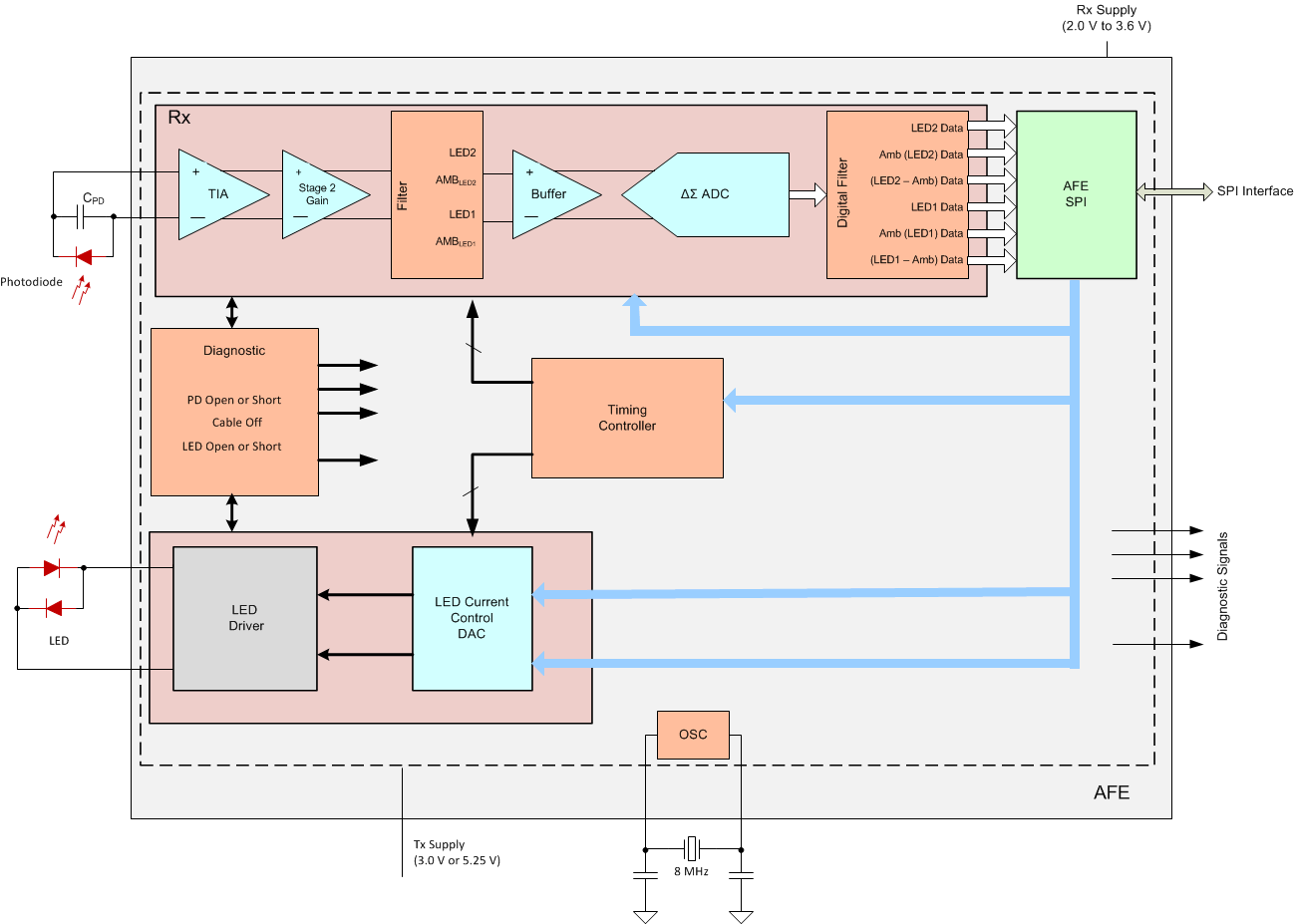
The AFE4490 is a fully-integrated analog front-end (AFE) that is ideally suited for pulse-oximeter applications. The device consists of a low-noise receiver channel with a 22-bit analog-to-digital converter (ADC), an LED transmit section, and diagnostics for sensor and LED fault detection. The device is a very configurable timing controller. This flexibility enables the user to have complete control of the device timing characteristics. To ease clocking requirements and provide a low-jitter clock to the device, an oscillator is also integrated that functions from an external crystal. The device communicates to an external microcontroller or host processor using an SPI™ interface.
The device is a complete AFE solution packaged in a single, compact VQFN-40 package (6 mm × 6 mm) and is specified over the operating temperature range of –40°C to 85°C.
Device Information(1)
| PART NUMBER | PACKAGE | BODY SIZE (NOM) |
|---|---|---|
| AFE4490 | VQFN (40) | 6.00 mm × 6.00 mm |
- For all available packages, see the orderable addendum at the end of the datasheet.