SBAS602H December 2012 – October 2014 AFE4490
PRODUCTION DATA.
- 1 Features
- 2 Applications
- 3 Description
- 4 Revision History
- 5 Device Comparison Table
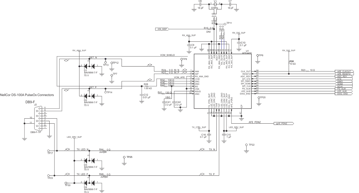
- 6 Pin Configuration and Functions
- 7 Specifications
- 8 Detailed Description
- 9 Applications and Implementation
- 10Power-Supply Recommendations
- 11Layout
- 12Device and Documentation Support
- 13Mechanical, Packaging, and Orderable Information
Package Options
Mechanical Data (Package|Pins)
- RHA|40
Thermal pad, mechanical data (Package|Pins)
Orderable Information
9 Applications and Implementation
NOTE
Information in the following applications sections is not part of the TI component specification, and TI does not warrant its accuracy or completeness. TI’s customers are responsible for determining suitability of components for their purposes. Customers should validate and test their design implementation to confirm system functionality.
9.1 Application Information
The AFE4490 can be used for measuring SPO2 and for monitoring heart rate. The high dynamic range of the device enables measuring SPO2 with a high degree of accuracy even under low-perfusion (ac-to-dc ratio) conditions. An SPO2 measurement system involves two different wavelength LEDs—usually Red and IR. By computing the ratio of the ac to dc at the two different wavelengths, the SPO2 can be calculated. Heart rate monitoring systems can also benefit from the high dynamic range of the device, which enables capturing a high-fidelity pulsating signal even in cases where the signal strength is low.
For more information on application guidelines, refer to the AFE44x0SPO2EVM User's Guide (SLAU480).
9.2 Typical Application
Device connections in a typical application are shown in Figure 131. Refer to the AFE44x0SPO2EVM User's Guide (SLAU480) for more details. The schematic in Figure 131 is a part of the AFE44x0SPO2EVM and shows a cabled application in which the LEDs and photodiode are connected to the AFE4490 through a cable. However, in an application without cables, the LEDs and photodiode can be directly connected to the TXP, TXN and INP, INN pins directly, as shown in the Design Requirements section.
TXM, TXP and INM, INP.
INM and INP must be guarded with VCM_SHIELD the signal. Run the VCM_SHIELD signal to the DB9 connector and back to the device.
9.2.1 Design Requirements
An SPO2 application usually involves a Red LED and an IR LED. These LEDs can be connected either in the common anode configuration or H-bridge configuration to the TXP, TXN pins. Figure 132 shows common anode configuration and Figure 133 shows H-bridge configuration.
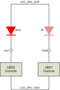 Figure 132. LEDs in Common Anode Configuration
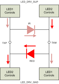 Figure 133. LEDs in H-Bridge Configuration
9.2.2 Detailed Design Procedure
The photodiode receives the light from both the Red and IR phases and usually has good sensitivities at both these wavelengths.
The photodiode connected in this manner operates in zero bias because of the negative feedback from the transimpedance amplifier. The connections of the photodiode to the AFE inputs are shown in Figure 134.
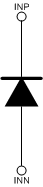 Figure 134. Photodiode Connection
The signal current generated by the photodiode is converted into a voltage by the transimpedance amplifier, which has a programmable transimpedance gain. The rest of the signal chain then presents a voltage to the ADC. The full-scale output of the transimpedance amplifier is ±1 V and the full-scale input to the ADC is ±1.2 V. An automatic gain control loop can be used to set the target dc voltage at the ADC input to approximately 50% of full scale. This type of AGC loop can control a combination of LED current and TIA gain to achieve this target value; see Figure 135.
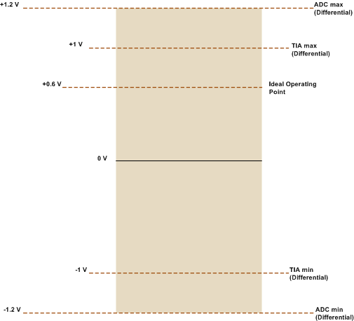 Figure 135. AGC Loop
The ADC output is a 22-bit code that is obtained by discarding the two MSBs of the 24-bit registers (for example the register with address 2Ah).
| D23 | D22 | D21 | D20 | D19 | D18 | D17 | D16 | D15 | D14 | D13 | D12 |
| Ignore | 22-Bit ADC Code, MSB to LSB | ||||||||||
| R/W-0h | R/W-0h | ||||||||||
| D11 | D10 | D9 | D8 | D7 | D6 | D5 | D4 | D3 | D2 | D1 | D0 |
| 22-Bit ADC Code, MSB to LSB | |||||||||||
| R/W-0h (TBD register correct?) | |||||||||||
| LEGEND: R/W = Read/Write; R = Read only; -n = value after reset |
Table 7 shows the mapping of the input voltage to the ADC output code.
Table 7. Input Voltage Mapping
| DIFFERENTIAL INPUT VOLTAGE AT ADC INPUT | 22-BIT ADC OUTPUT CODE |
|---|---|
| –1.2 V | 1000000000000000000000 |
| (–1.2 / 221) V | 1111111111111111111111 |
| 0 | 0000000000000000000000 |
| (1.2 / 221) V | 0000000000000000000001 |
| 1.2 V | 0111111111111111111111 |
The data format is binary twos complement format, MSB first. TI recommends that the input to the ADC does not exceed ±1 V (which is approximately 80% full-scale) because the TIA has a full-scale range of ±1 V.
9.2.3 Application Curve
The dc component of the current from the PPG signal is referred to as Pleth (short for photoplethysmography) current. The input-referred noise current (referred differentially to the INP, INN inputs) as a function of the Pleth current is shown in Figure 136 at a PRF of 600 Hz and for various duty cycles of LED pulsing. For example, a duty cycle of 25% refers to a case where the LED is pulsed for 25% of the pulse repetition period and the receiver samples the photodiode current for the same period of time. The noise shown in Figure 136 is the integrated noise over a 20-Hz bandwidth from dc.
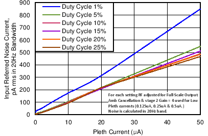 Figure 136. Input-Referred Noise Current vs
 Pleth Current (BW = 20Hz, PRF = 600 Hz)