SBAS602H December 2012 – October 2014 AFE4490
PRODUCTION DATA.
- 1 Features
- 2 Applications
- 3 Description
- 4 Revision History
- 5 Device Comparison Table
- 6 Pin Configuration and Functions
- 7 Specifications
- 8 Detailed Description
- 9 Applications and Implementation
- 10Power-Supply Recommendations
- 11Layout
- 12Device and Documentation Support
- 13Mechanical, Packaging, and Orderable Information
Package Options
Mechanical Data (Package|Pins)
- RHA|40
Thermal pad, mechanical data (Package|Pins)
Orderable Information
7 Specifications
7.1 Absolute Maximum Ratings
over operating free-air temperature range (unless otherwise noted)(1)| MIN | MAX | UNIT | ||
|---|---|---|---|---|
| RX_ANA_SUP, RX_DIG_SUP to RX_ANA_GND, RX_DIG_GND | –0.3 | 4 | V | |
| TX_CTRL_SUP, LED_DRV_SUP to LED_DRV_GND | –0.3 | 6 | V | |
| RX_ANA_GND, RX_DIG_GND to LED_DRV_GND | –0.3 | 0.3 | V | |
| Analog inputs | RX_ANA_GND – 0.3 | RX_ANA_SUP + 0.3 | V | |
| Digital inputs | RX_DIG_GND – 0.3 | RX_DIG_SUP + 0.3 | V | |
| TXP, TXN pins | –0.3 | Minimum [6, (LED_DRV_SUP + 0.3)] | V | |
| Input current to any pin except supply pins(2) | ±7 | mA | ||
| Input current | Momentary | ±50 | mA | |
| Continuous | ±7 | mA | ||
| Operating temperature range | –40 | 85 | °C | |
| Maximum junction temperature, TJ | 125 | °C | ||
(1) Stresses beyond those listed under Absolute Maximum Ratings may cause permanent damage to the device. These are stress ratings only, and do not imply functional operation of the device at these or any other conditions beyond those indicated under Recommended Operating Conditions. Exposure to absolute-maximum-rated conditions for extended periods may affect device reliability.
(2) Input pins are diode-clamped to the power-supply rails. Input signals that can swing beyond the supply rails must be current-limited to 10 mA or less.
7.2 Handling Ratings
| MIN | MAX | UNIT | |||
|---|---|---|---|---|---|
| Tstg | Storage temperature range | –60 | 150 | °C | |
| V(ESD) | Electrostatic discharge | Human body model (HBM), per ANSI/ESDA/JEDEC JS-001, all pins(1) | –1000 | 1000 | V |
| Charged device model (CDM), per JEDEC specification JESD22-C101, all pins(2) | –250 | 250 | |||
(1) JEDEC document JEP155 states that 500-V HBM allows safe manufacturing with a standard ESD control process.
(2) JEDEC document JEP157 states that 250-V CDM allows safe manufacturing with a standard ESD control process.
7.3 Recommended Operating Conditions
over operating free-air temperature range (unless otherwise noted)| MIN | MAX | UNIT | |||
|---|---|---|---|---|---|
| SUPPLIES | |||||
| RX_ANA_SUP | AFE analog supply | 2.0 | 3.6 | V | |
| RX_DIG_SUP | AFE digital supply | 2.0 | 3.6 | V | |
| TX_CTRL_SUP | Transmit controller supply | 3.0 | 5.25 | V | |
| LED_DRV_SUP | Transmit LED driver supply, H-bridge or common anode configuration | [3.0 or (VHR + VLED + VCABLE)(3)(1)(2), whichever is greater] | 5.25 | V | |
| Difference between LED_DRV_SUP and TX_CTRL_SUP | –0.3 | 0.3 | V | ||
| TEMPERATURE | |||||
| Specified temperature range | –40 | 85 | °C | ||
(1) VLED refers to the maximum voltage drop across the external LED (at maximum LED current) connected between the TXP and TXN pins (in H-bridge mode) and from the TXP and TXN pins to LED_DRV_SUP (in the common anode configuration).
(2) VCABLE refers to voltage drop across any cable, connector, or any other component in series with the LED.
(3) VHR refers to the required voltage headroom necessary to drive the LEDs. See Table 6 for the appropriate VHR value.
7.4 Thermal Information
| THERMAL METRIC(1) | AFE4490 | UNIT | |
|---|---|---|---|
| RHA (VQFN) | |||
| 40 PINS | |||
| RθJA | Junction-to-ambient thermal resistance | 35 | °C/W |
| RθJC(top) | Junction-to-case (top) thermal resistance | 31 | |
| RθJB | Junction-to-board thermal resistance | 26 | |
| ψJT | Junction-to-top characterization parameter | 0.1 | |
| ψJB | Junction-to-board characterization parameter | N/A | |
| RθJC(bot) | Junction-to-case (bottom) thermal resistance | N/A | |
(1) For more information about traditional and new thermal metrics, see the IC Package Thermal Metrics application report, SPRA953.
7.5 Electrical Characteristics
Minimum and maximum specifications are at TA = –40°C to 85°C. Typical specifications are at 25°C.All specifications are at RX_ANA_SUP = RX_DIG_SUP = 3 V, TX_CTRL_SUP = LED_DRV_SUP = 5 V, stage 2 amplifier disabled, and fCLK = 8 MHz, unless otherwise noted.
| PARAMETER | TEST CONDITIONS | MIN | TYP | MAX | UNIT | ||
|---|---|---|---|---|---|---|---|
| PERFORMANCE (Full-Signal Chain) | |||||||
| IIN_FS | Full-scale input current | RF = 10 kΩ | 50 | µA | |||
| RF = 25 kΩ | 20 | µA | |||||
| RF = 50 kΩ | 10 | µA | |||||
| RF = 100 kΩ | 5 | µA | |||||
| RF = 250 kΩ | 2 | µA | |||||
| RF = 500 kΩ | 1 | µA | |||||
| RF = 1 MΩ | 0.5 | µA | |||||
| PRF | Pulse repetition frequency | 62.5 | 5000 | SPS | |||
| DCPRF | PRF duty cycle | 25% | |||||
| CMRR | Common-mode rejection ratio | fCM = 50 Hz and 60 Hz, LED1 and LED2 with RSERIES = 500 kΩ, RF = 500 kΩ | 75 | dB | |||
| fCM = 50 Hz and 60 Hz, LED1-AMB and LED2-AMB with RSERIES = 500 kΩ, RF = 500 kΩ |
95 | dB | |||||
| PSRR | Power-supply rejection ratio | fPS = 50 Hz, 60 Hz at PRF = 200 Hz | 100 | dB | |||
| fCM = 50 Hz, 60 Hz at PRF = 600 Hz | 106 | dB | |||||
| PSRRLED | PSRR, transmit LED driver | With respect to ripple on LED_DRV_SUP | 75 | dB | |||
| PSRRTx | PSRR, transmit control | With respect to ripple on TX_CTRL_SUP | 60 | dB | |||
| PSRRRx | PSRR, receiver | With respect to ripple on RX_ANA_SUP and RX_DIG_SUP | 60 | dB | |||
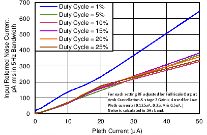
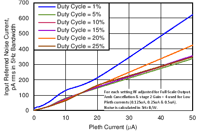
| Total integrated noise current, input-referred (receiver with transmitter loop back, 0.1-Hz to 20-Hz bandwidth) | RF = 100 kΩ with stage 2 gain disabled, PRF = 1200 Hz, duty cycle = 5% |
36 | pARMS | ||||
| RF = 500 kΩ with ambient cancellation enabled and stage 2 gain = 4, PRF = 1200 Hz, duty cycle = 25% |
13 | pARMS | |||||
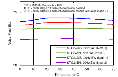
| NFB | Noise-free bits (receiver with transmitter loop back, 0.1-Hz to 20-Hz bandwidth)(1) | RF = 100 kΩ, PRF = 1200 Hz, duty cycle = 5% | 14.3 | Bits | |||
| RF = 500 kΩ, PRF = 1200 Hz, duty cycle = 25% | 13.5 | Bits | |||||
| RECEIVER FUNCTIONAL BLOCK LEVEL SPECIFICATION | |||||||
| Total integrated noise current, input-referred (receiver alone) over 0.1-Hz to 5-Hz bandwidth |
RF = 500 kΩ, ambient cancellation enabled, stage 2 gain = 4, PRF = 1300 Hz, LED duty cycle = 25% |
1.4 | pARMS | ||||
| RF = 500 kΩ, ambient cancellation enabled, stage 2 gain = 4, PRF = 1300 Hz, LED duty cycle = 5% |
5 | pARMS | |||||
| I-V TRANSIMPEDANCE AMPLIFIER | |||||||
| G | Gain | RF = 10 kΩ to RF = 1 MΩ | See the Receiver Channel section for details | V/µA | |||
| Gain accuracy | ±7% | ||||||
| Feedback resistance | RF | 10k, 25k, 50k, 100k, 250k, 500k, and 1M |
Ω | ||||
| Feedback resistor tolerance | RF | ±7% | |||||
| Feedback capacitance | CF | 5, 10, 25, 50, 100, and 250 | pF | ||||
| Feedback capacitor tolerance | CF | ±20% | |||||
| VOD(fs) | Full-scale differential output voltage | 1 | V | ||||
| Common-mode voltage on input pins | Set internally | 0.9 | V | ||||
| External differential input capacitance | Includes equivalent capacitance of photodiode, cables, EMI filter, and so forth | 10 | 1000 | pF | |||
| VO(shield) | Shield output voltage, VCM | With a 1-kΩ series resistor and a 10-nF decoupling capacitor to ground, when loaded with a small current (for example, of a few µA or less) | 0.8 | 0.9 | 1.0 | V | |
| AMBIENT CANCELLATION STAGE | |||||||
| G | Gain | 0, 3.5, 6, 9.5, and 12 | dB | ||||
| Current DAC range | 0 | 10 | µA | ||||
| Current DAC step size | 1 | µA | |||||
| LOW-PASS FILTER | |||||||
| Low-pass corner frequency | 3-dB attenuation | 0.5 and 1 | kHz | ||||
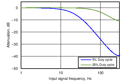
| Pass-band attenuation, 2 Hz to 10 Hz | Duty cycle = 25% | 0.004 | dB | ||||
| Duty cycle = 10% | 0.041 | dB | |||||
| Filter settling time | After diagnostics mode with filter corner = 500 Hz | 28 | ms | ||||
| After diagnostics mode with filter corner = 1000 Hz |
16 | ms | |||||
| ADC bypass outputs output impedance | RXOUTP and RXOUTN | 1 | kΩ | ||||
| ANALOG-TO-DIGITAL CONVERTER | |||||||
| Resolution | 22 | Bits | |||||
| Sample rate | See the ADC Operation and Averaging Module section | 4 × PRF | SPS | ||||
| ADC full-scale voltage | ±1.2 | V | |||||
| ADC conversion time | See the ADC Operation and Averaging Module section | 50 | PRF / 4 | µs | |||
| ADC reset time | 2 | tCLK | |||||
| TRANSMITTER | |||||||
| Output current range | 0, 50, 75, 100, 150, and 200 (see the LEDCNTRL: LED Control Register for details) |
mA | |||||
| LED current DAC error | ±5% | ||||||
| Output current resolution | 8 | Bits | |||||
| Transmitter noise dynamic range | 0.1-Hz to 20-Hz bandwidth, at 25-mA output current | 110 | dB | ||||
| 0.1-Hz to 20-Hz bandwidth, at 100-mA output current | 110 | dB | |||||
| Minimum sample time of LED1 and LED2 pulses | 50 | µs | |||||
| LED current DAC leakage current | LED_ON = 0 | 1 | µA | ||||
| LED_ON = 1 | 50 | µA | |||||
| LED current DAC linearity | Percent of full-scale current | 0.5% | |||||
| Output current settling time (with resistive load) |
From zero current to 150 mA | 7 | µs | ||||
| From 150 mA to zero current | 7 | µs | |||||
| DIAGNOSTICS | |||||||
| Duration of diagnostics state machine | EN_SLOW_DIAG = 0 Start of diagnostics after the DIAG_EN register bit is set. End of diagnostic indicated by DIAG_END going high. |
8 | ms | ||||
| EN_SLOW_DIAG = 1 Start of diagnostics after the DIAG_EN register bit is set. End of diagnostic indicated by DIAG_END going high. |
16 | ms | |||||
| Open fault resistance | > 100 | kΩ | |||||
| Short fault resistance | < 10 | kΩ | |||||
| Diagnostics current | During diagnostics mode | < 100 | µA | ||||
| INTERNAL OSCILLATOR | |||||||
| fCLKOUT | CLKOUT frequency | With an 8-MHz crystal connected to the XIN and XOUT pins | 4 | MHz | |||
| DCCLKOUT | CLKOUT duty cycle | 50% | |||||
| Crystal oscillator start-up time | With an 8-MHz crystal connected to the XIN and XOUT pins | 200 | µs | ||||
| EXTERNAL CLOCK | |||||||
| Maximum allowable external clock jitter | 50 | ps | |||||
| External clock input frequency | ±10% | 8 | MHz | ||||
| External clock input voltage | Voltage input high (VIH) | 0.75 × RX_DIG_SUP | V | ||||
| Voltage input low (VIL) | 0.25 × RX_DIG_SUP | V | |||||
| External clock input current | 1 | µA | |||||
| TIMING | |||||||
| Wake-up time from complete power-down | 1000 | ms | |||||
| Wake-up time from Rx power-down | 100 | µs | |||||
| Wake-up time from Tx power-down | 1000 | ms | |||||
| tRESET | Active low RESET pulse duration | 1 | ms | ||||
| tDIAGEND | DIAG_END pulse duration at diagnostics completion | 4 | CLKOUT cycles | ||||
| tADCRDY | ADC_RDY pulse duration | 1 | CLKOUT cycles | ||||
| DIGITAL SIGNAL CHARACTERISTICS | |||||||
| VIH | Logic high input voltage | AFE_PDN, SPI CLK, SPI SIMO, SPI STE, RESET | 0.75 × RX_DIG_SUP | V | |||
| VIL | Logic low input voltage | AFE_PDN, SPI CLK, SPI SIMO, SPI STE, RESET | 0.25 × RX_DIG_SUP | V | |||
| IIN | Logic input current | Digital inputs at VIH or VIL | 0.1 | µA | |||
| VOH | Logic high output voltage | DIAG_END, LED_ALM, PD_ALM, SPI SOMI, ADC_RDY, CLKOUT | RX_DIG_SUP – 0.1 | V | |||
| VOL | Logic low output voltage | DIAG_END, LED_ALM, PD_ALM, SPI SOMI, ADC_RDY, CLKOUT | 0.1 | V | |||
| PIN LEAKAGE CURRENT | |||||||
| Pin leakage current | To GND and supply | 1 | nA | ||||
| SUPPLY CURRENT | |||||||
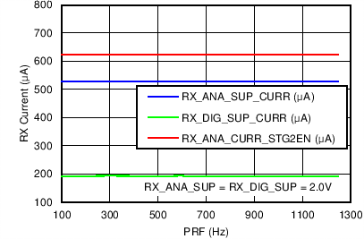
| Receiver analog supply current | RX_ANA_SUP = 3.0 V, with 8-MHz clock running, Rx stage 2 disabled | 0.6 | mA | ||||
| RX_ANA_SUP = 3.0 V, with 8-MHz clock running, Rx stage 2 enabled | 0.7 | mA | |||||
| Receiver digital supply current | RX_DIG_SUP = 3.0 V | 0.27 | mA | ||||
| ADC bypass mode | RX_ANA_SUP + RX_DIG_SUP (Excluding external ADC current) |
1.8 | mA | ||||
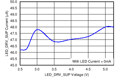
| LED_DRV_SUP | LED driver supply current | With zero LED current setting | 55 | µA | |||
| TX_CTRL_SUP | Transmitter control supply current | 15 | µA | ||||
| Complete power-down (using AFE_PDN pin) |
Receiver current only (RX_ANA_SUP) |
3 | µA | ||||
| Receiver current only (RX_DIG_SUP) |
3 | µA | |||||
| Transmitter current only (LED_DRV_SUP) |
1 | µA | |||||
| Transmitter current only (TX_CTRL_SUP) |
1 | µA | |||||
| Power-down Rx alone | Receiver current only (RX_ANA_SUP) |
220 | µA | ||||
| Receiver current only (RX_DIG_SUP) |
220 | µA | |||||
| Power-down Tx alone | Transmitter current only (LED_DRV_SUP) |
2 | µA | ||||
| Transmitter current only (TX_CTRL_SUP) |
2 | µA | |||||
| POWER DISSIPATION | |||||||
| PD(q) | Quiescent power dissipation | Normal operation (excluding LEDs) | 2.84 | mW | |||
| Power-down | 0.1 | mW | |||||
| Power-down with the AFE_PDN pin | LED_DRV_SUP | LED_DRV_SUP current value. Does not include LED current. |
1 | µA | |||
| TX_CTRL_SUP | 1 | µA | |||||
| RX_ANA_SUP | 5 | µA | |||||
| RX_DIG_SUP | 0.1 | µA | |||||
| Power-down with the PDNAFE register bit | LED_DRV_SUP | LED_DRV_SUP current value. Does not include LED current. |
1 | µA | |||
| TX_CTRL_SUP | 1 | µA | |||||
| RX_ANA_SUP | 15 | µA | |||||
| RX_DIG_SUP | 20 | µA | |||||
| Power-down Rx | LED_DRV_SUP | LED_DRV_SUP current value. Does not include LED current. |
50 | µA | |||
| TX_CTRL_SUP | 15 | µA | |||||
| RX_ANA_SUP | 220 | µA | |||||
| RX_DIG_SUP | 220 | µA | |||||
| Power-down Tx | LED_DRV_SUP | LED_DRV_SUP current value. Does not include LED current. |
2 | µA | |||
| TX_CTRL_SUP | 2 | µA | |||||
| RX_ANA_SUP | 600 | µA | |||||
| RX_DIG_SUP | 230 | µA | |||||
| After reset, with 8-MHz clock running | LED_DRV_SUP | LED_DRV_SUP current value. Does not include LED current. |
55 | µA | |||
| TX_CTRL_SUP | 15 | µA | |||||
| RX_ANA_SUP | 600 | µA | |||||
| RX_DIG_SUP | 230 | µA | |||||
| With stage 2 mode enabled and 8-MHz clock running | LED_DRV_SUP | LED_DRV_SUP current value. Does not include LED current. |
55 | µA | |||
| TX_CTRL_SUP | 15 | µA | |||||
| RX_ANA_SUP | 700 | µA | |||||
| RX_DIG_SUP | 270 | µA | |||||
(1) Noise-free bits (NFB) are defined as:
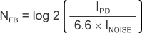
where: IPD is the photodiode current, and INOISE is the input-referred RMS noise current.
where: IPD is the photodiode current, and INOISE is the input-referred RMS noise current.
7.6 Timing Requirements: Serial Interface
| MIN | TYP | MAX | UNIT | ||
|---|---|---|---|---|---|
| tCLK | Clock frequency on XIN pin | 8 | MHz | ||
| tSCLK | Serial shift clock period | 62.5 | ns | ||
| tSTECLK | STE low to SCLK rising edge, setup time | 10 | ns | ||
| tCLKSTEH,L | SCLK transition to SPI STE high or low | 10 | ns | ||
| tSIMOSU | SIMO data to SCLK rising edge, setup time | 10 | ns | ||
| tSIMOHD | Valid SIMO data after SCLK rising edge, hold time | 10 | ns | ||
| tSOMIPD | SCLK falling edge to valid SOMI, setup time | 17 | ns | ||
| tSOMIHD | SCLK rising edge to invalid data, hold time | 0.5 | tSCLK | ||
1. The SPI_READ register bit must be enabled before attempting a register read.
2. Specify the register address whose contents must be read back on A[7:0].
3. The AFE outputs the contents of the specified register on the SOMI pin.
Figure 1. Serial Interface Timing Diagram, Read Operation123(1)(2)(3)
 Figure 2. Serial Interface Timing Diagram, Write Operation
7.7 Supply Ramp and Power-Down Timing Requirements
| VALUE | ||
|---|---|---|
| t1 | Time between Rx and Tx supplies ramping up | Keep as small as possible (for example, ±10 ms) |
| t2 | Time between both supplies stabilizing and high-going edge of RESET | > 100 ms |
| t3 | RESET pulse width | > 0.5 ms |
| t4 | Time between RESET and SPI commands | > 1 µs |
| t5 | Time between SPI commands and the ADC_RESET which corresponds to valid data | > 3 ms of cumulative sampling time in each phase(1)(2)(3) |
| t6 | Time between RESET pulse and high-accuracy data coming out of the signal chain | > 1 s(3) |
| t7 | Time from AFE_PDN high-going edge and RESET pulse(4) | > 100 ms |
| t8 | Time from AFE_PDN high-going edge (or PDN_AFE bit reset) to high-accuracy data coming out of the signal chain | > 1 s(3) |
(1) This time is required for each of the four switched RC filters to fully settle to the new settings. The same time is applicable whenever there is a change to any of the signal chain controls (for example, LED current setting, TIA gain, and so forth)
(2) If the SPI commands involve a change in the value of TX_REF from its default, then there is additional wait time that is approximately 1 s (for a 2.2-µF decoupling capacitor on the TX_REF pin).
(3) Dependent on the value of the capacitors on the BG and TX_REF pins. The 1-s wait time is necessary when the capacitors are 2.2 µF and scale down proportionate to the capacitor value. A very low capacitor (for example, 0.1 µF) on these pins causes the transmitter dynamic range to reduce to approximately 100 dB.
(4) After an active power-down from AFE_PDN, reset the device by using a low-going pulse on RESET.
 Figure 3. Supply Ramp and Hardware Power-Down Timing
 Figure 4. Supply Ramp and Software Power-Down Timing
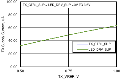
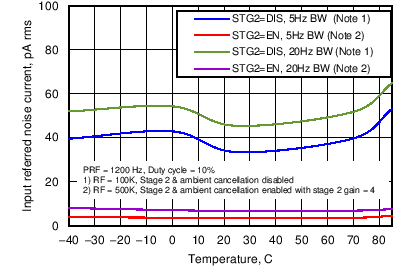
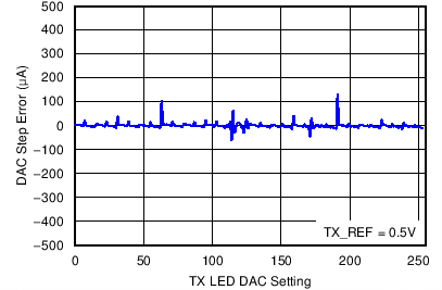
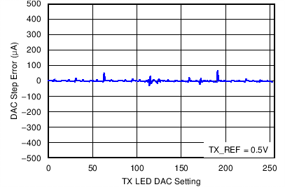
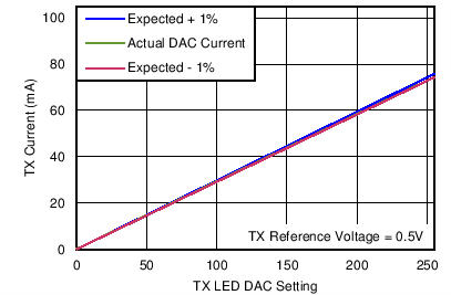
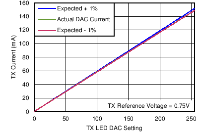
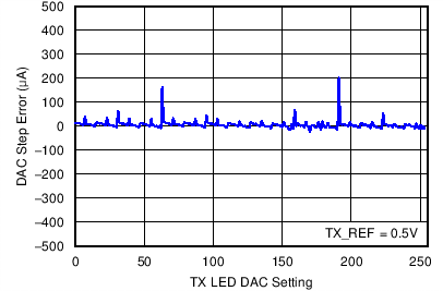
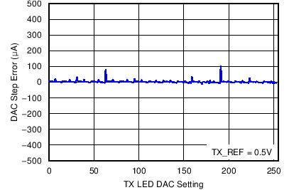
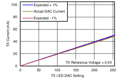
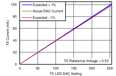
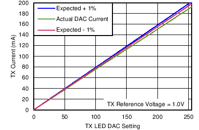
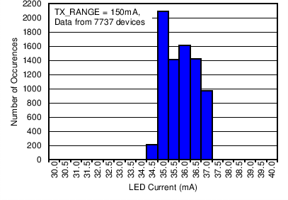
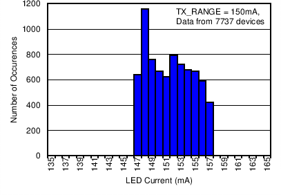
7.8 Typical Characteristics
At TA = 25°C, RX_ANA_SUP = RX_DIG_SUP = 3.0 V, TX_CTRL_SUP = LED_DRV_SUP = 5 V, and fCLK = 8 MHz, unless otherwise noted.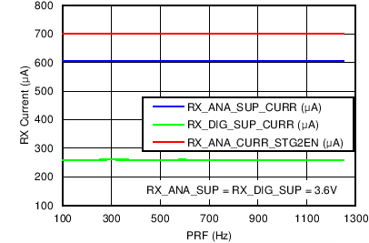
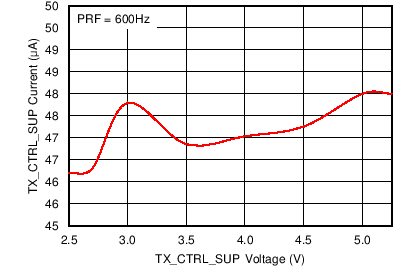
TX_CTRL_SUP Voltage
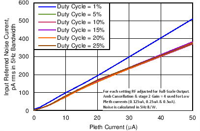
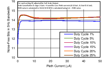
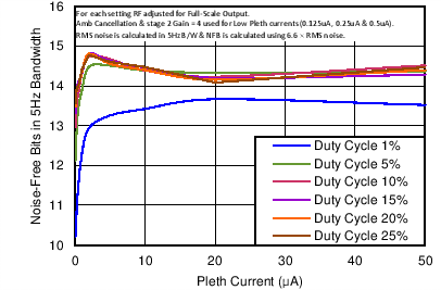
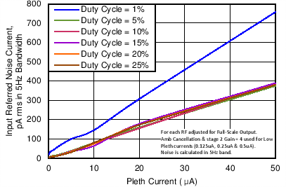
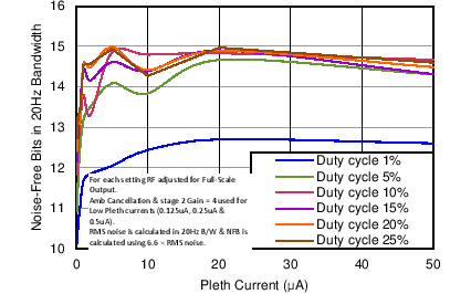
PLETH Current (BW = 5 Hz, PRF = 100 Hz)
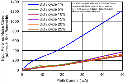
PLETH Current (BW = 5 Hz, PRF = 600 Hz)
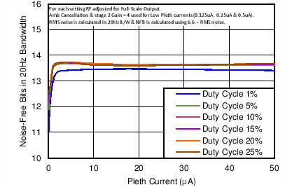
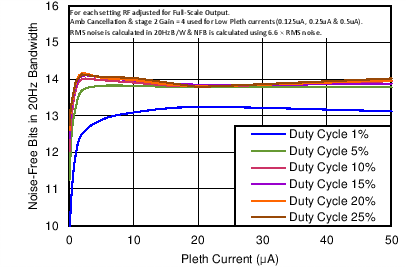
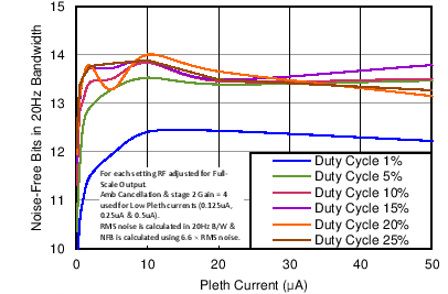
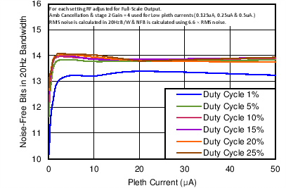
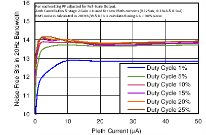
PLETH Current (BW = 20 Hz, PRF = 100 Hz)
PLETH Current (BW = 20 Hz, PRF = 600 Hz)
PLETH Current (BW = 5 Hz, PRF = 100 Hz)
PLETH Current (BW = 5 Hz, PRF = 600 Hz)
PLETH Current (BW = 20 Hz, PRF = 100 Hz)
PLETH Current (BW = 20 Hz, PRF = 600 Hz)
(5-Hz BW)
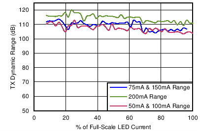
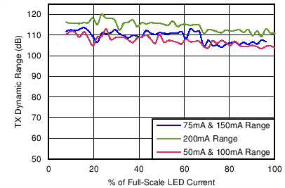
(200 mA, Max)
(100 mA, Max)
(50 mA, Max)
(75-mA Range)
(150-mA Range)
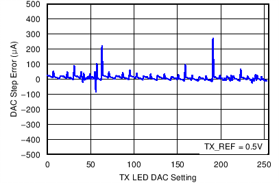
(10 mA)
(70 mA)
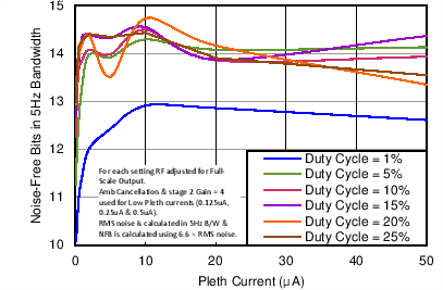
LED_DRV_SUP Voltage
PLETH Current (BW = 5 Hz, PRF = 300 Hz)
PLETH Current (BW = 5 Hz, PRF = 1200 Hz)
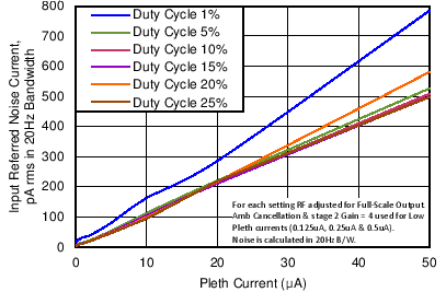
PLETH Current (BW = 20 Hz, PRF = 300 Hz)
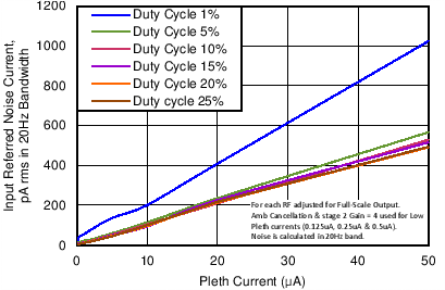
PLETH Current (BW = 20 Hz, PRF = 1200 Hz)
PLETH Current (BW = 5 Hz, PRF = 300 Hz)
PLETH Current (BW = 20 Hz, PRF = 300 Hz)
(20-Hz BW)
(150 mA, Max)
(50-mA Range)
(100-mA Range)
(200-mA Range)
(35 mA)
(150 mA)