SBOS927B May 2019 – October 2021 ALM2402F-Q1
PRODUCTION DATA
- 1 Features
- 2 Applications
- 3 Description
- 4 Revision History
- 5 Pin Configuration and Functions
- 6 Specifications
- 7 Detailed Description
- 8 Application and Implementation
- 9 Power Supply Recommendations
- 10Layout
- 11Device and Documentation Support
- 12Mechanical, Packaging, and Orderable Information
Package Options
Mechanical Data (Package|Pins)
- PWP|14
Thermal pad, mechanical data (Package|Pins)
- PWP|14
Orderable Information
7.3.4 Input Common-Mode Overvoltage Clamps
The input common mode range of the ALM2402F-Q1 is between (V–) + 0.2 V and (V+) – 1.2 V (see the Electrical Characteristics table). Staying within this range allows the op amps to perform and operate within the specification listed in the Electrical Characteristics. Operating beyond these limits can cause distortion and nonlinearities.
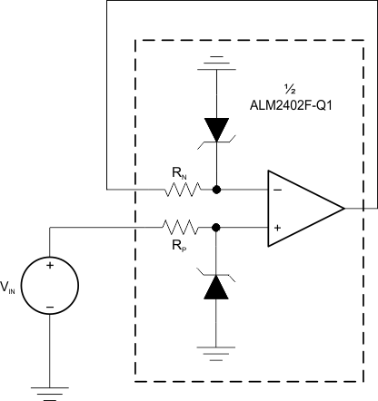
In order for the inputs to tolerate high voltages in the event of a short to supply, Zener diodes have been added (see Figure 7-1). The current into this Zener diode is limited through internal resistors (10 kΩ each). When operating near or above the Zener voltage (7 V), the additional voltage error caused by the mismatch in internal resistors must be taken in to account. In unity gain configurations, the op amp forces both gate voltages to be equal to the Zener voltage on the positive input pin, and ideally both Zeners sink the same amount of current and force the output voltage to be equal to VIN. However, in reality, RN and RP and VZ between both Zener diodes do not perfectly match, and have some percentage difference between their values. This occurrence leads to the output being VO = VIN × (ΔR + ΔVZ) .
 Figure 7-1 Schematic Including Input Clamps