SBOS927B May   2019  – October 2021 ALM2402F-Q1

PRODUCTION DATA  

  1. Features
  2. Applications
  3. Description
  4. Revision History
  5. Pin Configuration and Functions
  6. Specifications
    1. 6.1 Absolute Maximum Ratings
    2. 6.2 ESD Ratings
    3. 6.3 Recommended Operating Conditions
    4. 6.4 Thermal Information
    5. 6.5 Electrical Characteristics: VS = 12 V
    6. 6.6 Electrical Characteristics: VS = 5 V
    7. 6.7 Typical Characteristics
  7. Detailed Description
    1. 7.1 Overview
    2. 7.2 Functional Block Diagram
    3. 7.3 Feature Description
      1. 7.3.1 OTF/SH_DN
      2. 7.3.2 Output Stage Supply Voltage
      3. 7.3.3 Current-Limit and Short-Circuit Protection
      4. 7.3.4 Input Common-Mode Overvoltage Clamps
      5. 7.3.5 Thermal Shutdown
      6. 7.3.6 Output Stage
      7. 7.3.7 EMI Susceptibility and Input Filtering
    4. 7.4 Device Functional Modes
      1. 7.4.1 Open-Loop and Closed-Loop Operation
      2. 7.4.2 Shutdown
  8. Application and Implementation
    1. 8.1 Application Information
      1. 8.1.1 Capacitive Load and Stability
    2. 8.2 Typical Application
      1. 8.2.1 Design Requirements
      2. 8.2.2 Detailed Design Procedure
        1. 8.2.2.1 Resolver Excitation Input (Op Amp Output)
          1. 8.2.2.1.1 Excitation Voltage
          2. 8.2.2.1.2 Excitation Frequency
          3. 8.2.2.1.3 Excitation Impedance
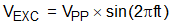
        2. 8.2.2.2 Resolver Output
        3. 8.2.2.3 Power Dissipation and Thermal Reliability
          1. 8.2.2.3.1 Improving Package Thermal Performance
      3. 8.2.3 Application Curves
  9. Power Supply Recommendations
  10. 10Layout
    1. 10.1 Layout Guidelines
    2. 10.2 Layout Example
  11. 11Device and Documentation Support
    1. 11.1 Documentation Support
      1. 11.1.1 Related Documentation
    2. 11.2 Receiving Notification of Documentation Updates
    3. 11.3 Support Resources
    4. 11.4 Trademarks
    5. 11.5 Electrostatic Discharge Caution
    6. 11.6 Glossary
  12. 12Mechanical, Packaging, and Orderable Information

Package Options

Mechanical Data (Package|Pins)
Thermal pad, mechanical data (Package|Pins)
Orderable Information

Resolver Output

As mentioned in Section 8.2.2.1.2, the excitation signal is similar to a sampling pulse in ADCs, with the real information being in the envelope created by the rotor. Equation 3, Equation 4, and Equation 5 show the behavior of the sin and cos outputs. The excitation signal is attenuated and enveloped by the voltage created from the electromagnetic response of the rotating rotor. The resolver analog-output-to-digital converter filters out the excitation signal, and processes the sine and cosine angles produced by the rotor. Hence, signal integrity or the sine and cosine envelope is most important in resolver design; although, some trade-offs in signal integrity of the excitation signal can be made for cost or convenience. Often, a square wave or sawtooth signal is used to accomplish excitation, as opposed to a sine wave.

Equation 3. GUID-A56D844B-164A-4179-BBD6-F08ABBDFB6FD-low.gif
Equation 4. GUID-C42519CD-30E8-4379-A661-EC355D3F7AC9-low.gif
Equation 5. GUID-2BC73EA2-B682-404C-86B6-9F8488225CA0-low.gif