SPRS999 August 2017 AM5718-HIREL
PRODUCTION DATA.
- 1 Device Overview
- 2 Revision History
- 3 Device Comparison
-
4 Terminal Configuration and Functions
- 4.1 Terminal Assignment
- 4.2 Ball Characteristics
- 4.3 Multiplexing Characteristics
- 4.4
Signal Descriptions
- 4.4.1 Video Input Ports (VIP)
- 4.4.2 Display Subsystem - Video Output Ports
- 4.4.3 Display Subsystem - High-Definition Multimedia Interface (HDMI)
- 4.4.4 Camera Serial Interface 2 CAL bridge (CSI2)
- 4.4.5 External Memory Interface (EMIF)
- 4.4.6 General-Purpose Memory Controller (GPMC)
- 4.4.7 Timers
- 4.4.8 Inter-Integrated Circuit Interface (I2C)
- 4.4.9 HDQ / 1-Wire Interface (HDQ1W)
- 4.4.10 Universal Asynchronous Receiver Transmitter (UART)
- 4.4.11 Multichannel Serial Peripheral Interface (McSPI)
- 4.4.12 Quad Serial Peripheral Interface (QSPI)
- 4.4.13 Multichannel Audio Serial Port (McASP)
- 4.4.14 Universal Serial Bus (USB)
- 4.4.15 SATA
- 4.4.16 Peripheral Component Interconnect Express (PCIe)
- 4.4.17 Controller Area Network Interface (DCAN)
- 4.4.18 Ethernet Interface (GMAC_SW)
- 4.4.19 Media Local Bus (MLB) Interface
- 4.4.20 eMMC/SD/SDIO
- 4.4.21 General-Purpose Interface (GPIO)
- 4.4.22 Keyboard controller (KBD)
- 4.4.23 Pulse Width Modulation (PWM) Interface
- 4.4.24 Programmable Real-Time Unit Subsystem and Industrial Communication Subsystem (PRU-ICSS)
- 4.4.25 Test Interfaces
- 4.4.26 System and Miscellaneous
- 4.4.27 Power Supplies
-
5 Specifications
- 5.1 Absolute Maximum Ratings
- 5.2 ESD Ratings
- 5.3 Power On Hours (POH) Limits
- 5.4 Recommended Operating Conditions
- 5.5 Operating Performance Points
- 5.6 Power Consumption Summary
- 5.7
Electrical Characteristics
- 5.7.1 LVCMOS DDR DC Electrical Characteristics
- 5.7.2 HDMIPHY DC Electrical Characteristics
- 5.7.3 Dual Voltage LVCMOS I2C DC Electrical Characteristics
- 5.7.4 IQ1833 Buffers DC Electrical Characteristics
- 5.7.5 IHHV1833 Buffers DC Electrical Characteristics
- 5.7.6 LVCMOS OSC Buffers DC Electrical Characteristics
- 5.7.7 LVCMOS CSI2 DC Electrical Characteristics
- 5.7.8 BMLB18 Buffers DC Electrical Characteristics
- 5.7.9 BC1833IHHV Buffers DC Electrical Characteristics
- 5.7.10 USBPHY DC Electrical Characteristics
- 5.7.11 Dual Voltage SDIO1833 DC Electrical Characteristics
- 5.7.12 Dual Voltage LVCMOS DC Electrical Characteristics
- 5.7.13 SATAPHY DC Electrical Characteristics
- 5.7.14 SERDES DC Electrical Characteristics
- 5.8 Thermal Characteristics
- 5.9 Power Supply Sequences
- 6 Clock Specifications
-
7 Timing Requirements and Switching Characteristics
- 7.1 Timing Test Conditions
- 7.2 Interface Clock Specifications
- 7.3 Timing Parameters and Information
- 7.4 Recommended Clock and Control Signal Transition Behavior
- 7.5 Virtual and Manual I/O Timing Modes
- 7.6 Video Input Ports (VIP)
- 7.7 Display Subsystem - Video Output Ports
- 7.8 Display Subsystem - High-Definition Multimedia Interface (HDMI)
- 7.9 Camera Serial Interface 2 CAL bridge (CSI2)
- 7.10 External Memory Interface (EMIF)
- 7.11 General-Purpose Memory Controller (GPMC)
- 7.12 Timers
- 7.13 Inter-Integrated Circuit Interface (I2C)
- 7.14 HDQ / 1-Wire Interface (HDQ1W)
- 7.15 Universal Asynchronous Receiver Transmitter (UART)
- 7.16 Multichannel Serial Peripheral Interface (McSPI)
- 7.17 Quad Serial Peripheral Interface (QSPI)
- 7.18 Multichannel Audio Serial Port (McASP)
- 7.19 Universal Serial Bus (USB)
- 7.20 Serial Advanced Technology Attachment (SATA)
- 7.21 Peripheral Component Interconnect Express (PCIe)
- 7.22 Controller Area Network Interface (DCAN)
- 7.23 Ethernet Interface (GMAC_SW)
- 7.24
eMMC/SD/SDIO
- 7.24.1
MMC1-SD Card Interface
- 7.24.1.1 Default speed, 4-bit data, SDR, half-cycle
- 7.24.1.2 High speed, 4-bit data, SDR, half-cycle
- 7.24.1.3 SDR12, 4-bit data, half-cycle
- 7.24.1.4 SDR25, 4-bit data, half-cycle
- 7.24.1.5 UHS-I SDR50, 4-bit data, half-cycle
- 7.24.1.6 UHS-I SDR104, 4-bit data, half-cycle
- 7.24.1.7 UHS-I DDR50, 4-bit data
- 7.24.2 MMC2 - eMMC
- 7.24.3 MMC3 and MMC4-SDIO/SD
- 7.24.1
MMC1-SD Card Interface
- 7.25 General-Purpose Interface (GPIO)
- 7.26 PRU-ICSS Interfaces
- 7.27 System and Miscellaneous interfaces
- 7.28 Test Interfaces
-
8 Applications, Implementation, and Layout
- 8.1 Power Supply Mapping
- 8.2
DDR3 Board Design and Layout Guidelines
- 8.2.1 DDR3 General Board Layout Guidelines
- 8.2.2
DDR3 Board Design and Layout Guidelines
- 8.2.2.1 Board Designs
- 8.2.2.2 DDR3 EMIF
- 8.2.2.3 DDR3 Device Combinations
- 8.2.2.4 DDR3 Interface Schematic
- 8.2.2.5 Compatible JEDEC DDR3 Devices
- 8.2.2.6 PCB Stackup
- 8.2.2.7 Placement
- 8.2.2.8 DDR3 Keepout Region
- 8.2.2.9 Bulk Bypass Capacitors
- 8.2.2.10 High-Speed Bypass Capacitors
- 8.2.2.11 Net Classes
- 8.2.2.12 DDR3 Signal Termination
- 8.2.2.13 VREF_DDR Routing
- 8.2.2.14 VTT
- 8.2.2.15 CK and ADDR_CTRL Topologies and Routing Definition
- 8.2.2.16 Data Topologies and Routing Definition
- 8.2.2.17 Routing Specification
- 8.3 High Speed Differential Signal Routing Guidance
- 8.4 Power Distribution Network Implementation Guidance
- 8.5 Single-Ended Interfaces
- 8.6 Clock Routing Guidelines
- 9 Device and Documentation Support
- 10Mechanical Packaging and Orderable Information
Package Options
Mechanical Data (Package|Pins)
- ZBO|760
Thermal pad, mechanical data (Package|Pins)
Orderable Information
8 Applications, Implementation, and Layout
NOTE
Information in the following Applications section is not part of the TI component specification, and TI does not warrant its accuracy or completeness. TI's customers are responsible for determining suitability of components for their purposes. Customers should validate and test their design implementation to confirm system functionality.
8.1 Power Supply Mapping
TPS65916 or TPS659037 are the Power Management ICs (PMICs) that should be used for the Device designs. TI requires use of these PMICs for the following reasons:
- TI has validated their use with the Device
- Board level margins including transient response and output accuracy are analyzed and optimized for the entire system
- Support for power sequencing requirements (refer to Section 5.9 Power Supply Sequences)
- Support for Adaptive Voltage Scaling (AVS) Class 0 requirements, including TI provided software
Whenever we allow for combining of rails mapped on any of the SMPSes, the PDN guidelines that are the most stringent of the rails combined should be implemented for the particular supply rail.
It is possible that some voltage domains on the device are unused in some systems. In such cases, to ensure device reliability, it is still required that the supply pins for the specific voltage domains are connected to some core power supply output.
These unused supplies though can be combined with any of the core supplies that are used (active) in the system. e.g. if IVA and GPU domains are not used, they can be combined with the CORE domain, thereby having a single power supply driving the combined CORE, IVA and GPU domains.
For the combined rail, the following relaxations do apply:
- The AVS voltage of active rail in the combined rail needs to be used to set the power supply
- The decoupling capacitance should be set according to the active rail in the combined rail
Table 8-1 illustrates the approved and validated power supply connections to the Device for the SMPS outputs of the TPS659037 PMIC.
Table 8-1 TPS659037 Power Supply Connections(1)
| TPS659037 POWER SUPPLY | VALID COMBINATION 1: |
VALID COMBINATION 2: |
|---|---|---|
| SMPS1/2(2) | vdd_mpu | vdd_mpu |
| SMPS3 | vdds_ddr1 | vdds_ddr1 |
| SMPS4/5 | vdd_dsp, vdd_gpu, vdd_iva | vdd_dsp |
| SMPS6 | vdd | vdd_gpu |
| SMPS7 | SW configuration after boot | vdd |
| SMPS8 | vdds18v | vdd_iva |
| SMPS9 | SW configuration after boot 3.3V | vddshvx |
| LDO1 | vddshv8 | vddshv8 |
| LDO2 | vddshv5 | vdds18v |
| LDO3 | vdda_usb1, vdda_usb2, vdda_csi,vdda_sata | vdda_usb1, vdda_usb2, vdda_csi, vdda_sata |
| LDO4 | vdda_hdmi, vdda_pcie, vdda_pcie0, vdda_usb3 | vdda_hdmi, vdda_pcie, vdda_pcie0, vdda_usb3 |
| LDO9 | vdd_rtc | vdd_rtc |
| LDOLN | 1.8V PLLs | 1.8V PLLs |
| LDOUSB | vdda_usb3v3 | vdda_usb3v3 |
- Power consumption is highly application-specific. Separate analysis must be performed to ensure output current ratings (average and peak) is within the limits of the PMIC for all rails of the device.
- Refer to the PMIC data manual for the latest TPS659037 specifications.
- For more information on connectivity with the TPS659037 PMIC, see the TPS659037 User’s Guide to Power AM572x (SLIU011).
- A product’s maximum ambient temperature, thermal system design & heat spreading performance could limit the maximum power dissipation below the full PMIC capacity in order to not exceed recommended SoC max Tj.
Table 8-2 illustrates the approved and validated power supply connections to the Device for the SMPS outputs of the TPS65916 PMIC.
Table 8-2 TPS65916 Power Supply Connections
| TPS65916 POWER SUPPLY | VALID COMBINATION 1: |
|---|---|
| SMPS1 | vdd_mpu |
| SMPS2 | vdd |
| SMPS3 | vdd_dsp, vdd_gpu, vdd_iva |
| SMPS4 | vdds18v |
| SMPS5 | vdds_ddr1 |
8.2 DDR3 Board Design and Layout Guidelines
8.2.1 DDR3 General Board Layout Guidelines
To help ensure good signaling performance, consider the following board design guidelines:
- Avoid crossing splits in the power plane.
- Minimize Vref noise.
- Use the widest trace that is practical between decoupling capacitors and memory module.
- Maintain a single reference.
- Minimize ISI by keeping impedances matched.
- Minimize crosstalk by isolating sensitive bits, such as strobes, and avoiding return path discontinuities.
- Use proper low-pass filtering on the Vref pins.
- Keep the stub length as short as possible.
- Add additional spacing for on-clock and strobe nets to eliminate crosstalk.
- Maintain a common ground reference for all bypass and decoupling capacitors.
- Take into account the differences in propagation delays between microstrip and stripline nets when evaluating timing constraints.
8.2.2 DDR3 Board Design and Layout Guidelines
8.2.2.1 Board Designs
TI only supports board designs using DDR3 memory that follow the guidelines in this document. The switching characteristics and timing diagram for the DDR3 memory controller are shown in Table 8-3 and Figure 8-1.
Table 8-3 Switching Characteristics Over Recommended Operating Conditions for DDR3 Memory Controller
| NO. | PARAMETER | MIN | MAX | UNIT | |
|---|---|---|---|---|---|
| 1 | tc(DDR_CLK) | Cycle time, DDR_CLK | 1.5 | 2.5(1) | ns |
- This is the absolute maximum the clock period can be. Actual maximum clock period may be limited by DDR3 speed grade and operating frequency (see the DDR3 memory device data sheet).
 Figure 8-1 DDR3 Memory Controller Clock Timing
8.2.2.2 DDR3 EMIF
The processor contains one DDR3 EMIF.
8.2.2.3 DDR3 Device Combinations
Because there are several possible combinations of device counts and single- or dual-side mounting, Table 8-4 summarizes the supported device configurations.
Table 8-4 Supported DDR3 Device Combinations
| NUMBER OF DDR3 DEVICES | DDR3 DEVICE WIDTH (BITS) | MIRRORED? | DDR3 EMIF WIDTH (BITS) |
|---|---|---|---|
| 1 | 16 | N | 16 |
| 2 | 8 | Y(1) | 16 |
| 2 | 16 | N | 32 |
| 2 | 16 | Y(1) | 32 |
| 3 | 16 | N (3) | 32 |
| 4 | 8 | N | 32 |
| 4 | 8 | Y(2) | 32 |
| 5 | 8 | N (3) | 32 |
- Two DDR3 devices are mirrored when one device is placed on the top of the board and the second device is placed on the bottom of the board.
- This is two mirrored pairs of DDR3 devices.
- Three or five DDR3 device combination is not available on this device, but combination types are retained for consistency with the AM57xx family of devices.
8.2.2.4 DDR3 Interface Schematic
8.2.2.4.1 32-Bit DDR3 Interface
The DDR3 interface schematic varies, depending upon the width of the DDR3 devices used and the width of the bus used (16 or 32 bits). General connectivity is straightforward and very similar. 16-bit DDR devices look like two 8-bit devices. Figure 8-2 and Figure 8-3 show the schematic connections for 32-bit interfaces using x16 devices.
8.2.2.4.2 16-Bit DDR3 Interface
Note that the 16-bit wide interface schematic is practically identical to the 32-bit interface (see Figure 8-2 and Figure 8-3); only the high-word DDR memories are removed and the unused DQS inputs are tied off.
When not using all or part of a DDR interface, the proper method of handling the unused pins is to tie off the ddrx_dqsi pins to ground via a 1k-Ω resistor and to tie off the ddrx_dqsni pins to the corresponding vdds_ddrx supply via a 1k-Ω resistor. This needs to be done for each byte not used. Although these signals have internal pullups and pulldowns, external pullups and pulldowns provide additional protection against external electrical noise causing activity on the signals.
The vdds_ddrx and ddrx_vref0 power supply pins need to be connected to their respective power supplies even if ddrx is not being used. All other DDR interface pins can be left unconnected. Note that the supported modes for use of the DDR EMIF are 32-bits wide, 16-bits wide, or not used.
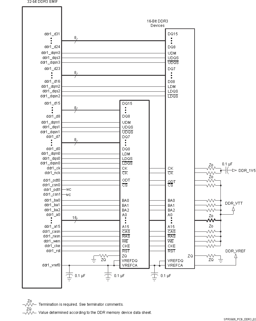 Figure 8-2 32-Bit, One-Bank DDR3 Interface Schematic Using Two 16-Bit DDR3 Devices
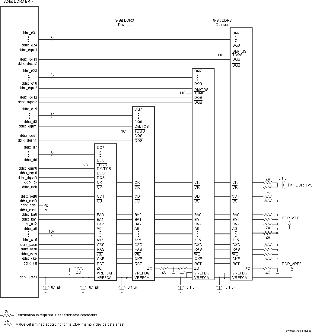 Figure 8-3 32-Bit, One-Bank DDR3 Interface Schematic Using Four 8-Bit DDR3 Devices
8.2.2.5 Compatible JEDEC DDR3 Devices
Table 8-5 shows the parameters of the JEDEC DDR3 devices that are compatible with this interface. Generally, the DDR3 interface is compatible with DDR3-1333 devices in the x8 or x16 widths.
Table 8-5 Compatible JEDEC DDR3 Devices (Per Interface)
| NO. | PARAMETER | CONDITION | MIN | MAX | UNIT |
|---|---|---|---|---|---|
| 1 | JEDEC DDR3 device speed grade(1) | DDR clock rate = 400MHz | DDR3-800 | DDR3-1600 | |
| 400MHz< DDR clock rate ≤ 533MHz | DDR3-1066 | DDR3-1600 | |||
| 533MHz < DDR clock rate ≤ 667MHz | DDR3-1333 | DDR3-1600 | |||
| 2 | JEDEC DDR3 device bit width | x8 | x16 | Bits | |
| 3 | JEDEC DDR3 device count(2) | 2 | 4 | Devices |
- Refer to Table 8-3 Switching Characteristics Over Recommended Operating Conditions for DDR3 Memory Controller for the range of supported DDR clock rates.
- For valid DDR3 device configurations and device counts, see Section 8.2.2.4, Figure 8-2, and Figure 8-3.
8.2.2.6 PCB Stackup
The minimum stackup for routing the DDR3 interface is a six-layer stack up as shown in Table 8-6. Additional layers may be added to the PCB stackup to accommodate other circuitry, enhance SI/EMI performance, or to reduce the size of the PCB footprint. Complete stackup specifications are provided in Table 8-7.
Table 8-6 Six-Layer PCB Stackup Suggestion
| LAYER | TYPE | DESCRIPTION |
|---|---|---|
| 1 | Signal | Top routing mostly vertical |
| 2 | Plane | Ground |
| 3 | Plane | Split power plane |
| 4 | Plane | Split power plane or Internal routing |
| 5 | Plane | Ground |
| 6 | Signal | Bottom routing mostly horizontal |
Table 8-7 PCB Stackup Specifications
| NO. | PARAMETER | MIN | TYP | MAX | UNIT |
|---|---|---|---|---|---|
| PS1 | PCB routing/plane layers | 6 | |||
| PS2 | Signal routing layers | 3 | |||
| PS3 | Full ground reference layers under DDR3 routing region(1) | 1 | |||
| PS4 | Full 1.5-V power reference layers under the DDR3 routing region(1) | 1 | |||
| PS5 | Number of reference plane cuts allowed within DDR routing region(2) | 0 | |||
| PS6 | Number of layers between DDR3 routing layer and reference plane(3) | 0 | |||
| PS7 | PCB routing feature size | 4 | Mils | ||
| PS8 | PCB trace width, w | 4 | Mils | ||
| PS9 | Single-ended impedance, Zo | 50 | 75 | Ω | |
| PS10 | Impedance control(5) | Z-5 | Z | Z+5 | Ω |
- Ground reference layers are preferred over power reference layers. Be sure to include bypass caps to accommodate reference layer return current as the trace routes switch routing layers.
- No traces should cross reference plane cuts within the DDR routing region. High-speed signal traces crossing reference plane cuts create large return current paths which can lead to excessive crosstalk and EMI radiation.
- Reference planes are to be directly adjacent to the signal plane to minimize the size of the return current loop.
- An 18-mil pad assumes Via Channel is the most economical BGA escape. A 20-mil pad may be used if additional layers are available for power routing. An 18-mil pad is required for minimum layer count escape.
- Z is the nominal singled-ended impedance selected for the PCB specified by PS9.
8.2.2.7 Placement
Figure 8-4 shows the required placement for the processor as well as the DDR3 devices. The dimensions for this figure are defined in Table 8-8. The placement does not restrict the side of the PCB on which the devices are mounted. The ultimate purpose of the placement is to limit the maximum trace lengths and allow for proper routing space. For a 16-bit DDR memory system, the high-word DDR3 devices are omitted from the placement.
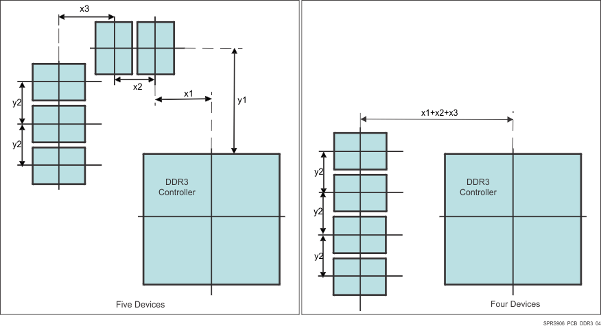 Figure 8-4 Placement Specifications
Table 8-8 Placement Specifications DDR3
| NO. | PARAMETER | MIN | MAX | UNIT |
|---|---|---|---|---|
| KOD31 | X1 | 500 | Mils | |
| KOD32 | X2 | 600 | Mils | |
| KOD33 | X3 | 600 | Mils | |
| KOD34 | Y1 | 1800 | Mils | |
| KOD35 | Y2 | 600 | Mils | |
| KOD36 | DDR3 keepout region (1) | |||
| KOD37 | Clearance from non-DDR3 signal to DDR3 keepout region (2) (3) | 4 | W |
- DDR3 keepout region to encompass entire DDR3 routing area.
- Non-DDR3 signals allowed within DDR3 keepout region provided they are separated from DDR3 routing layers by a ground plane.
- If a device has more than one DDR controller, the signals from the other controller(s) are considered non-DDR3 and should be separated by this specification.
8.2.2.8 DDR3 Keepout Region
The region of the PCB used for DDR3 circuitry must be isolated from other signals. The DDR3 keepout region is defined for this purpose and is shown in Figure 8-5. The size of this region varies with the placement and DDR routing. Additional clearances required for the keepout region are shown in Table 8-8. Non-DDR3 signals should not be routed on the DDR signal layers within the DDR3 keepout region. Non-DDR3 signals may be routed in the region, provided they are routed on layers separated from the DDR signal layers by a ground layer. No breaks should be allowed in the reference ground layers in this region. In addition, the 1.5-V DDR3 power plane should cover the entire keepout region. Also note that the two signals from the DDR3 controller should be separated from each other by the specification in Table 8-8, (see KOD37).
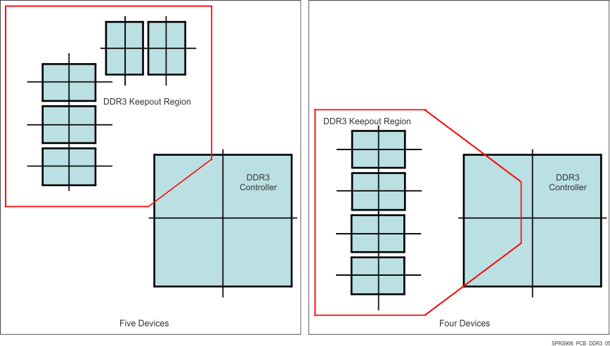 Figure 8-5 DDR3 Keepout Region
8.2.2.9 Bulk Bypass Capacitors
Bulk bypass capacitors are required for moderate speed bypassing of the DDR3 and other circuitry. Table 8-9 contains the minimum numbers and capacitance required for the bulk bypass capacitors. Note that this table only covers the bypass needs of the DDR3 controllers and DDR3 devices. Additional bulk bypass capacitance may be needed for other circuitry.
Table 8-9 Bulk Bypass Capacitors
| NO. | PARAMETER | MIN | MAX | UNIT |
|---|---|---|---|---|
| 1 | vdds_ddrx bulk bypass capacitor count(1) | 1 | Devices | |
| 2 | vdds_ddrx bulk bypass total capacitance | 22 | μF |
- These devices should be placed near the devices they are bypassing, but preference should be given to the placement of the high-speed (HS) bypass capacitors and DDR3 signal routing.
8.2.2.10 High-Speed Bypass Capacitors
High-speed (HS) bypass capacitors are critcal for proper DDR3 interface operation. It is particularly important to minimize the parasitic series inductance of the HS bypass capacitors, processor/DDR power, and processor/DDR ground connections. Table 8-10 contains the specification for the HS bypass capacitors as well as for the power connections on the PCB. Generally speaking, it is good to:
- Fit as many HS bypass capacitors as possible.
- Minimize the distance from the bypass cap to the pins/balls being bypassed.
- Use the smallest physical sized capacitors possible with the highest capacitance readily available.
- Connect the bypass capacitor pads to their vias using the widest traces possible and using the largest hole size via possible.
- Minimize via sharing. Note the limites on via sharing shown in Table 8-10.
Table 8-10 High-Speed Bypass Capacitors
| NO. | PARAMETER | MIN | TYP | MAX | UNIT |
|---|---|---|---|---|---|
| 1 | HS bypass capacitor package size(1) | 0201 | 0402 | 10 Mils | |
| 2 | Distance, HS bypass capacitor to processor being bypassed(2)(3)(4) | 400 | Mils | ||
| 3 | Processor HS bypass capacitor count per vdds_ddrx rail | See Section 8.4 and (11) | Devices | ||
| 4 | Processor HS bypass capacitor total capacitance per vdds_ddrx rail | See Section 8.4 and (11) | μF | ||
| 5 | Number of connection vias for each device power/ground ball(5) | Vias | |||
| 6 | Trace length from device power/ground ball to connection via(2) | 35 | 70 | Mils | |
| 7 | Distance, HS bypass capacitor to DDR device being bypassed(6) | 150 | Mils | ||
| 8 | DDR3 device HS bypass capacitor count(7) | 12 | Devices | ||
| 9 | DDR3 device HS bypass capacitor total capacitance(7) | 0.85 | μF | ||
| 10 | Number of connection vias for each HS capacitor(8)(9) | 2 | Vias | ||
| 11 | Trace length from bypass capacitor connect to connection via(2)(9) | 35 | 100 | Mils | |
| 12 | Number of connection vias for each DDR3 device power/ground ball(10) | 1 | Vias | ||
| 13 | Trace length from DDR3 device power/ground ball to connection via(2)(8) | 35 | 60 | Mils | |
- LxW, 10-mil units, that is, a 0402 is a 40x20-mil surface-mount capacitor.
- Closer/shorter is better.
- Measured from the nearest processor power/ground ball to the center of the capacitor package.
- Three of these capacitors should be located underneath the processor, between the cluster of DDR_1V5 balls and ground balls, between the DDR interfaces on the package.
- See the Via Channel™ escape for the processor package.
- Measured from the DDR3 device power/ground ball to the center of the capacitor package.
- Per DDR3 device.
- An additional HS bypass capacitor can share the connection vias only if it is mounted on the opposite side of the board. No sharing of vias is permitted on the same side of the board.
- An HS bypass capacitor may share a via with a DDR device mounted on the same side of the PCB. A wide trace should be used for the connection and the length from the capacitor pad to the DDR device pad should be less than 150 mils.
- Up to a total of two pairs of DDR power/ground balls may share a via.
- The capacitor recommendations in this data manual reflect only the needs of this processor. Please see the memory vendor’s guidelines for determining the appropriate decoupling capacitor arrangement for the memory device itself.
8.2.2.10.1 Return Current Bypass Capacitors
Use additional bypass capacitors if the return current reference plane changes due to DDR3 signals hopping from one signal layer to another. The bypass capacitor here provides a path for the return current to hop planes along with the signal. As many of these return current bypass capacitors should be used as possible. Because these are returns for signal current, the signal via size may be used for these capacitors.
8.2.2.11 Net Classes
Table 8-11 lists the clock net classes for the DDR3 interface. Table 8-12 lists the signal net classes, and associated clock net classes, for signals in the DDR3 interface. These net classes are used for the termination and routing rules that follow.
Table 8-11 Clock Net Class Definitions
| CLOCK NET CLASS | Processor PIN NAMES |
|---|---|
| CK | ddrx_ck/ddrx_nck |
| DQS0 | ddrx_dqs0 / ddrx_dqsn0 |
| DQS1 | ddrx_dqs1 / ddrx_dqsn1 |
| DQS2(1) | ddrx_dqs2 / ddrx_dqsn2 |
| DQS3(1) | ddrx_dqs3 / ddrx_dqsn3 |
- Only used on 32-bit wide DDR3 memory systems.
Table 8-12 Signal Net Class Definitions
| SIGNAL NET CLASS | ASSOCIATED CLOCK NET CLASS |
Processor PIN NAMES |
|---|---|---|
| ADDR_CTRL | CK | ddrx_ba[2:0], ddrx_a[14:0], ddrx_csnj, ddrx_casn, ddrx_rasn, ddrx_wen, ddrx_cke, ddrx_odti |
| DQ0 | DQS0 | ddrx_d[7:0], ddrx_dqm0 |
| DQ1 | DQS1 | ddrx_d[15:8], ddrx_dqm1 |
| DQ2(1) | DQS2 | ddrx_d[23:16], ddrx_dqm2 |
| DQ3(1) | DQS3 | ddrx_d[31:24], ddrx_dqm3 |
- Only used on 32-bit wide DDR3 memory systems.
8.2.2.12 DDR3 Signal Termination
Signal terminators are required for the CK and ADDR_CTRL net classes. The data lines are terminated by ODT and, thus, the PCB traces should be unterminated. Detailed termination specifications are covered in the routing rules in the following sections.
8.2.2.13 VREF_DDR Routing
ddrx_vref0 (VREF) is used as a reference by the input buffers of the DDR3 memories as well as the processor. VREF is intended to be half the DDR3 power supply voltage and is typically generated with the DDR3 VDDS and VTT power supply. It should be routed as a nominal 20-mil wide trace with 0.1 µF bypass capacitors near each device connection. Narrowing of VREF is allowed to accommodate routing congestion.
8.2.2.14 VTT
Like VREF, the nominal value of the VTT supply is half the DDR3 supply voltage. Unlike VREF, VTT is expected to source and sink current, specifically the termination current for the ADDR_CTRL net class Thevinen terminators. VTT is needed at the end of the address bus and it should be routed as a power sub-plane. VTT should be bypassed near the terminator resistors.
8.2.2.15 CK and ADDR_CTRL Topologies and Routing Definition
The CK and ADDR_CTRL net classes are routed similarly and are length matched to minimize skew between them. CK is a bit more complicated because it runs at a higher transition rate and is differential. The following subsections show the topology and routing for various DDR3 configurations for CK and ADDR_CTRL. The figures in the following subsections define the terms for the routing specification detailed in Table 8-13.
8.2.2.15.1 Four DDR3 Devices
Four DDR3 devices are supported on the DDR EMIF consisting of four x8 DDR3 devices arranged as one bank (CS). These four devices may be mounted on a single side of the PCB, or may be mirrored in two pairs to save board space at a cost of increased routing complexity and parts on the backside of the PCB.
8.2.2.15.1.1 CK and ADDR_CTRL Topologies, Four DDR3 Devices
Figure 8-6 shows the topology of the CK net classes and Figure 8-7 shows the topology for the corresponding ADDR_CTRL net classes.
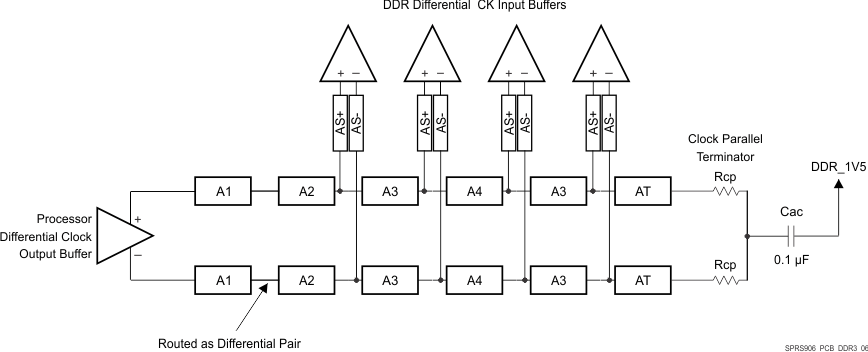 Figure 8-6 CK Topology for Four x8 DDR3 Devices
 Figure 8-7 ADDR_CTRL Topology for Four x8 DDR3 Devices
8.2.2.15.1.2 CK and ADDR_CTRL Routing, Four DDR3 Devices
Figure 8-8 shows the CK routing for four DDR3 devices placed on the same side of the PCB. Figure 8-9 shows the corresponding ADDR_CTRL routing.
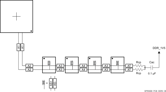 Figure 8-8 CK Routing for Four Single-Side DDR3 Devices
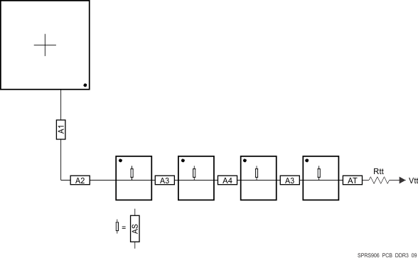 Figure 8-9 ADDR_CTRL Routing for Four Single-Side DDR3 Devices
To save PCB space, the four DDR3 memories may be mounted as two mirrored pairs at a cost of increased routing and assembly complexity. Figure 8-10 and Figure 8-11 show the routing for CK and ADDR_CTRL, respectively, for four DDR3 devices mirrored in a two-pair configuration.
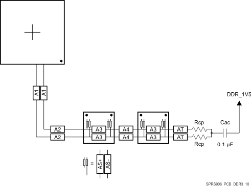 Figure 8-10 CK Routing for Four Mirrored DDR3 Devices
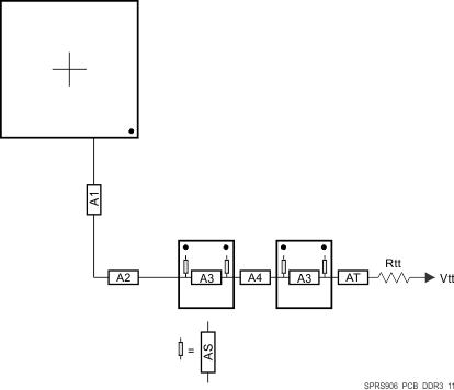 Figure 8-11 ADDR_CTRL Routing for Four Mirrored DDR3 Devices
8.2.2.15.2 Two DDR3 Devices
Two DDR3 devices are supported on the DDR EMIF consisting of two x8 DDR3 devices arranged as one bank (CS), 16 bits wide, or two x16 DDR3 devices arranged as one bank (CS), 32 bits wide. These two devices may be mounted on a single side of the PCB, or may be mirrored in a pair to save board space at a cost of increased routing complexity and parts on the backside of the PCB.
8.2.2.15.2.1 CK and ADDR_CTRL Topologies, Two DDR3 Devices
Figure 8-12 shows the topology of the CK net classes and Figure 8-13 shows the topology for the corresponding ADDR_CTRL net classes.
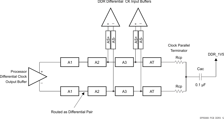 Figure 8-12 CK Topology for Two DDR3 Devices
 Figure 8-13 ADDR_CTRL Topology for Two DDR3 Devices
8.2.2.15.2.2 CK and ADDR_CTRL Routing, Two DDR3 Devices
Figure 8-14 shows the CK routing for two DDR3 devices placed on the same side of the PCB. Figure 8-15 shows the corresponding ADDR_CTRL routing.
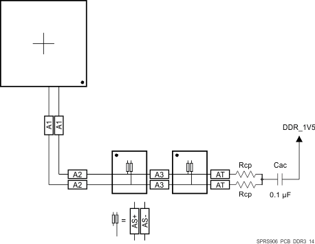 Figure 8-14 CK Routing for Two Single-Side DDR3 Devices
 Figure 8-15 ADDR_CTRL Routing for Two Single-Side DDR3 Devices
To save PCB space, the two DDR3 memories may be mounted as a mirrored pair at a cost of increased routing and assembly complexity. Figure 8-16 and Figure 8-17 show the routing for CK and ADDR_CTRL, respectively, for two DDR3 devices mirrored in a single-pair configuration.
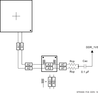 Figure 8-16 CK Routing for Two Mirrored DDR3 Devices
 Figure 8-17 ADDR_CTRL Routing for Two Mirrored DDR3 Devices
8.2.2.15.3 One DDR3 Device
A single DDR3 device is supported on the DDR EMIF consisting of one x16 DDR3 device arranged as one bank (CS), 16 bits wide.
8.2.2.15.3.1 CK and ADDR_CTRL Topologies, One DDR3 Device
Figure 8-18 shows the topology of the CK net classes and Figure 8-19 shows the topology for the corresponding ADDR_CTRL net classes.
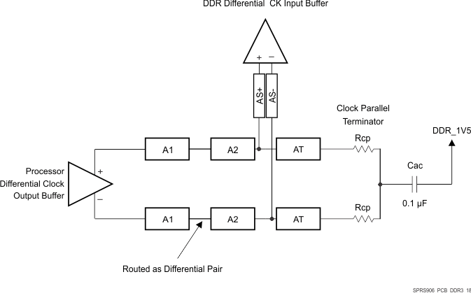 Figure 8-18 CK Topology for One DDR3 Device
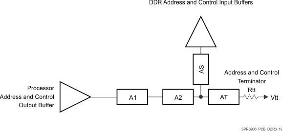 Figure 8-19 ADDR_CTRL Topology for One DDR3 Device
8.2.2.15.3.2 CK and ADDR/CTRL Routing, One DDR3 Device
Figure 8-20 shows the CK routing for one DDR3 device placed on the same side of the PCB. Figure 8-21 shows the corresponding ADDR_CTRL routing.
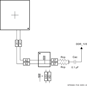 Figure 8-20 CK Routing for One DDR3 Device
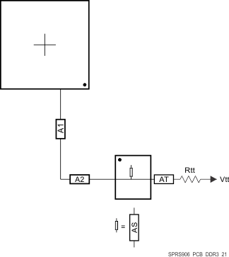 Figure 8-21 ADDR_CTRL Routing for One DDR3 Device
8.2.2.16 Data Topologies and Routing Definition
No matter the number of DDR3 devices used, the data line topology is always point to point, so its definition is simple.
Care should be taken to minimize layer transitions during routing. If a layer transition is necessary, it is better to transition to a layer using the same reference plane. If this cannot be accommodated, ensure there are nearby ground vias to allow the return currents to transition between reference planes if both reference planes are ground or vdds_ddr. Ensure there are nearby bypass capacitors to allow the return currents to transition between reference planes if one of the reference planes is ground. The goal is to minimize the size of the return current loops.
8.2.2.16.1 DQS and DQ/DM Topologies, Any Number of Allowed DDR3 Devices
DQS lines are point-to-point differential, and DQ/DM lines are point-to-point singled ended. Figure 8-22 and Figure 8-23 show these topologies.
 Figure 8-22 DQS Topology
 Figure 8-23 DQ/DM Topology
8.2.2.16.2 DQS and DQ/DM Routing, Any Number of Allowed DDR3 Devices
Figure 8-24 and Figure 8-25 show the DQS and DQ/DM routing.
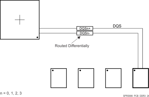 Figure 8-24 DQS Routing With Any Number of Allowed DDR3 Devices
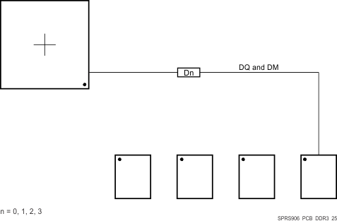 Figure 8-25 DQ/DM Routing With Any Number of Allowed DDR3 Devices
8.2.2.17 Routing Specification
8.2.2.17.1 CK and ADDR_CTRL Routing Specification
Skew within the CK and ADDR_CTRL net classes directly reduces setup and hold margin and, thus, this skew must be controlled. The only way to practically match lengths on a PCB is to lengthen the shorter traces up to the length of the longest net in the net class and its associated clock. A metric to establish this maximum length is Manhattan distance. The Manhattan distance between two points on a PCB is the length between the points when connecting them only with horizontal or vertical segments. A reasonable trace route length is to within a percentage of its Manhattan distance. CACLM is defined as Clock Address Control Longest Manhattan distance.
Given the clock and address pin locations on the processor and the DDR3 memories, the maximum possible Manhattan distance can be determined given the placement. Figure 8-26 and Figure 8-27 show this distance for four loads and two loads, respectively. It is from this distance that the specifications on the lengths of the transmission lines for the address bus are determined. CACLM is determined similarly for other address bus configurations; that is, it is based on the longest net of the CK/ADDR_CTRL net class. For CK and ADDR_CTRL routing, these specifications are contained in Table 8-13.
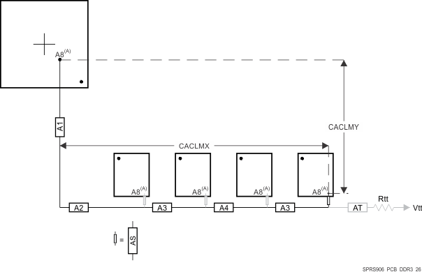
The length of shorter CK/ADDR_CTRL stubs as well as the length of the terminator stub are not included in this length calculation. Non-included lengths are grayed out in the figure.
Assuming A8 is the longest, CALM = CACLMY + CACLMX + 300 mils.
The extra 300 mils allows for routing down lower than the DDR3 memories and returning up to reach A8.
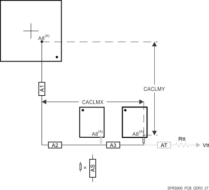
Table 8-13 CK and ADDR_CTRL Routing Specification(2)(3)
| NO. | PARAMETER | MIN | TYP | MAX | UNIT |
|---|---|---|---|---|---|
| CARS31 | A1+A2 length | 500(1) | ps | ||
| CARS32 | A1+A2 skew | 29 | ps | ||
| CARS33 | A3 length | 125 | ps | ||
| CARS34 | A3 skew(4) | 6 | ps | ||
| CARS35 | A3 skew(5) | 6 | ps | ||
| CARS36 | A4 length | 125 | ps | ||
| CARS37 | A4 skew | 6 | ps | ||
| CARS38 | AS length | 5(1) | 17 | ps | |
| CARS39 | AS skew | 1.3(1) | 14 | ps | |
| CARS310 | AS+/AS- length | 5 | 12 | ps | |
| CARS311 | AS+/AS- skew | 1 | ps | ||
| CARS312 | AT length(6) | 75 | ps | ||
| CARS313 | AT skew(7) | 14 | ps | ||
| CARS314 | AT skew(8) | 1 | ps | ||
| CARS315 | CK/ADDR_CTRL trace length | 1020 | ps | ||
| CARS316 | Vias per trace | 3(1) | vias | ||
| CARS317 | Via count difference | 1(15) | vias | ||
| CARS318 | Center-to-center CK to other DDR3 trace spacing(9) | 4w | |||
| CARS319 | Center-to-center ADDR_CTRL to other DDR3 trace spacing(9)(10) | 4w | |||
| CARS320 | Center-to-center ADDR_CTRL to other ADDR_CTRL trace spacing(9) | 3w | |||
| CARS321 | CK center-to-center spacing(11) (12) | ||||
| CARS322 | CK spacing to other net(9) | 4w | |||
| CARS323 | Rcp(13) | Zo-1 | Zo | Zo+1 | Ω |
| CARS324 | Rtt(13)(14) | Zo-5 | Zo | Zo+5 | Ω |
- Max value is based upon conservative signal integrity approach. This value could be extended only if detailed signal integrity analysis of rice time and fall time confirms desired operation.
- The use of vias should be minimized.
- Additional bypass capacitors are required when using the DDR_1V5 plane as the reference plane to allow the return current to jump between the DDR_1V5 plane and the ground plane when the net class switches layers at a via.
- Non-mirrored configuration (all DDR3 memories on same side of PCB).
- Mirrored configuration (one DDR3 device on top of the board and one DDR3 device on the bottom).
- While this length can be increased for convenience, its length should be minimized.
- ADDR_CTRL net class only (not CK net class). Minimizing this skew is recommended, but not required.
- CK net class only.
- Center-to-center spacing is allowed to fall to minimum 2w for up to 1250 mils of routed length.
- The ADDR_CTRL net class of the other DDR EMIF is considered other DDR3 trace spacing.
- CK spacing set to ensure proper differential impedance.
- The most important thing to do is control the impedance so inadvertent impedance mismatches are not created. Generally speaking, center-to-center spacing should be either 2w or slightly larger than 2w to achieve a differential impedance equal to twice the singleended impedance, Zo.
- Source termination (series resistor at driver) is specifically not allowed.
- Termination values should be uniform across the net class.
- Via count difference may increase by 1 only if accurate 3-D modeling of the signal flight times – including accurately modeled signal propagation through vias – has been applied to ensure all segment skew maximums are not exceeded.
8.2.2.17.2 DQS and DQ Routing Specification
Skew within the DQS and DQ/DM net classes directly reduces setup and hold margin and thus this skew must be controlled. The only way to practically match lengths on a PCB is to lengthen the shorter traces up to the length of the longest net in the net class and its associated clock. As with CK and ADDR_CTRL, a reasonable trace route length is to within a percentage of its Manhattan distance. DQLMn is defined as DQ Longest Manhattan distance n, where n is the byte number. For a 32-bit interface, there are four DQLMs, DQLM0-DQLM3. Likewise, for a 16-bit interface, there are two DQLMs, DQLM0-DQLM1.
NOTE
It is not required, nor is it recommended, to match the lengths across all bytes. Length matching is only required within each byte.
Given the DQS and DQ/DM pin locations on the processor and the DDR3 memories, the maximum possible Manhattan distance can be determined given the placement. Figure 8-28 shows this distance for four loads. It is from this distance that the specifications on the lengths of the transmission lines for the data bus are determined. For DQS and DQ/DM routing, these specifications are contained in Table 8-14.
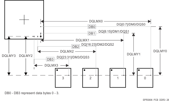
DQLM0 = DQLMX0 + DQLMY0
DQLM1 = DQLMX1 + DQLMY1
DQLM2 = DQLMX2 + DQLMY2
DQLM3 = DQLMX3 + DQLMY3
Table 8-14 Data Routing Specification(2)
| NO. | PARAMETER | MIN | TYP | MAX | UNIT |
|---|---|---|---|---|---|
| DRS31 | DB0 length | 340 | ps | ||
| DRS32 | DB1 length | 340 | ps | ||
| DRS33 | DB2 length | 340 | ps | ||
| DRS34 | DB3 length | 340 | ps | ||
| DRS35 | DBn skew(3) | 5 | ps | ||
| DRS36 | DQSn+ to DQSn- skew | 1 | ps | ||
| DRS37 | DQSn to DBn skew(3)(4) | 5(10) | ps | ||
| DRS38 | Vias per trace | 2(1) | vias | ||
| DRS39 | Via count difference | 0(10) | vias | ||
| DRS310 | Center-to-center DBn to other DDR3 trace spacing(6) | 4 | w(5) | ||
| DRS311 | Center-to-center DBn to other DBn trace spacing(7) | 3 | w(5) | ||
| DRS312 | DQSn center-to-center spacing(8) (9) | ||||
| DRS313 | DQSn center-to-center spacing to other net | 4 | w(5) |
- Max value is based upon conservative signal integrity approach. This value could be extended only if detailed signal integrity analysis of rice time and fall time confirms desired operation.
- External termination disallowed. Data termination should use built-in ODT functionality.
- Length matching is only done within a byte. Length matching across bytes is neither required nor recommended.
- Each DQS pair is length matched to its associated byte.
- Center-to-center spacing is allowed to fall to minimum 2w for up to 1250 mils of routed length.
- Other DDR3 trace spacing means other DDR3 net classes not within the byte.
- This applies to spacing within the net classes of a byte.
- DQS pair spacing is set to ensure proper differential impedance.
- The most important thing to do is control the impedance so inadvertent impedance mismatches are not created. Generally speaking, center-to-center spacing should be either 2w or slightly larger than 2w to achieve a differential impedance equal to twice the singleended impedance, Zo.
- Via count difference may increase by 1 only if accurate 3-D modeling of the signal flight times – including accurately modeled signal propagation through vias – has been applied to ensure DBn skew and DQSn to DBn skew maximums are not exceeded.
8.3 High Speed Differential Signal Routing Guidance
The High-Speed Interface Layout Guidelines Application Report (SPRAAR7) available from http://www.ti.com/lit/pdf/spraar7 provides guidance for successful routing of the high speed differential signals. This includes PCB stackup and materials guidance as well as routing skew, length and spacing limits. TI supports only designs that follow the board design guidelines contained in the application report.
8.4 Power Distribution Network Implementation Guidance
The Power Distribution Network Implementation Guidelines Application Report (SPRABY8) available from http://www.ti.com/lit/pdf/spraby8 provides guidance for successful implementation of the power distribution network. This includes PCB stackup guidance as well as guidance for optimizing the selection and placement of the decoupling capacitors. TI supports only designs that follow the board design guidelines contained in the application report.
8.5 Single-Ended Interfaces
8.5.1 General Routing Guidelines
The following paragraphs detail the routing guidelines that must be observed when routing the various functional LVCMOS interfaces.
- Line spacing:
- For a line width equal to W, the spacing between two lines must be 2W, at least. This minimizes the crosstalk between switching signals between the different lines. On the PCB, this is not achievable everywhere (for example, when breaking signals out from the device package), but it is recommended to follow this rule as much as possible. When violating this guideline, minimize the length of the traces running parallel to each other (see Figure 8-29).
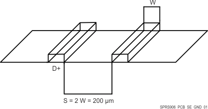 Figure 8-29 Ground Guard Illustration
- Length matching (unless otherwise specified):
- For bus or traces at frequencies less than 10 MHz, the trace length matching (maximum length difference between the longest and the shortest lines) must be less than 25 mm.
- For bus or traces at frequencies greater than 10 MHz, the trace length matching (maximum length difference between the longest and the shortest lines) must be less than 2.5 mm.
- Characteristic impedance
- Unless otherwise specified, the characteristic impedance for single-ended interfaces is recommended to be between 35-Ω and 65-Ω.
- Multiple peripheral support
- For interfaces where multiple peripherals have to be supported in the star topology, the length of each branch has to be balanced. Before closing the PCB design, it is highly recommended to verify signal integrity based on simulations including actual PCB extraction.
8.5.2 QSPI Board Design and Layout Guidelines
The following section details the routing guidelines that must be observed when routing the QSPI interfaces.
- The qspi1_sclk output signal must be looped back into the qspi1_rtclk input.
- The signal propagation delay from the qspi1_sclk ball to the QSPI device CLK input pin (A to C) must be approximately equal to the signal propagation delay from the QSPI device CLK pin to the qspi1_rtclk ball (C to D).
- The signal propagation delay from the QSPI device CLK pin to the qspi1_rtclk ball (C to D) must be approximately equal to the signal propagation delay of the control and data signals between the QSPI device and the SoC device (E to F, or F to E).
- The signal propagation delay from the qspi1_sclk signal to the series terminators (R2 = 10 Ω) near the QSPI device must be < 450pS (~7cm as stripline or ~8cm as microstrip)
- 50 Ω PCB routing is recommended along with series terminations, as shown in Figure 8-30.
- Propagation delays and matching:
- A to C = C to D = E to F.
- Matching skew: < 60pS
- A to B < 450pS
- B to C = as small as possible (<60pS)
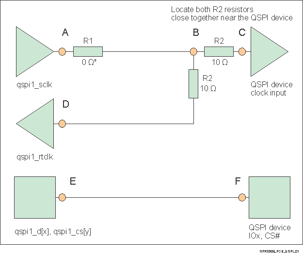 Figure 8-30 QSPI Interface High Level Schematic
NOTE
*0 Ω resistor (R1), located as close as possible to the qspi1_sclk pin, is placeholder for fine-tuning if needed.
8.6 Clock Routing Guidelines
8.6.1 32-kHz Oscillator Routing
When designing the printed-circuit board:
- Keep the crystal as close as possible to the crystal pins X1 and X2.
- Keep the trace lengths short and small to reduce capacitor loading and prevent unwanted noise pickup.
- Place a guard ring around the crystal and tie the ring to ground to help isolate the crystal from unwanted noise pickup.
- Keep all signals out from beneath the crystal and the X1 and X2 pins to prevent noise coupling.
- Finally, an additional local ground plane on an adjacent PCB layer can be added under the crystal to shield it from unwanted pickup from traces on other layers of the board. This plane must be isolated from the regular PCB ground plane and tied to the GND pin of the RTC. The plane must not be any larger than the perimeter of the guard ring. Make sure that this ground plane does not contribute to significant capacitance (a few pF) between the signal line and ground on the connections that run from X1 and X2 to the crystal.
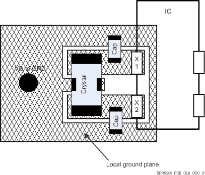 Figure 8-31 Slow Clock PCB Requirements
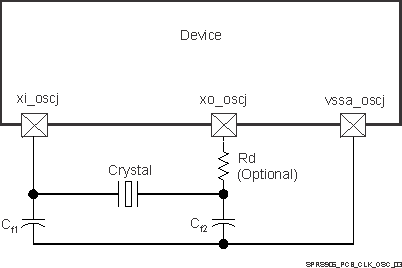
8.6.2 Oscillator Ground Connection
Although the impedance of a ground plane is low it is, of course, not zero. Therefore, any noise current in the ground plane causes a voltage drop in the ground. Figure 8-32 shows the grounding scheme for slow (low frequency) clock generated from the internal oscillator.
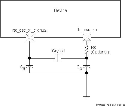 Figure 8-32 Grounding Scheme for Low-Frequency Clock
Figure 8-33 shows the grounding scheme for high-frequency clock.
