| QUIESCENT CURRENTS |
| IBAT |
Battery discharge current (BAT, SW, SYS) in buck mode |
VBAT = 4.5 V, VBUS < VAC-UVLOZ, leakage between BAT and VBUS, TJ< 85°C |
|
|
5 |
µA |
| IBAT |
Battery discharge current (BAT) in buck mode |
VBAT = 4.5 V, HIZ Mode and OVPFET_DIS = 1 or No VBUS, I2C disabled, BATFET Disabled. TJ < 85°C |
|
17 |
33 |
µA |
| IBAT |
Battery discharge current (BAT, SW, SYS) |
VBAT = 4.5 V, HIZ Mode and OVPFET_DIS = 1 or No VBUS, I2C Disabled, BATFET Enabled. TJ < 85°C |
|
58 |
85 |
µA |
| IVAC_HIZ |
Input supply current (VAC) in buck mode |
VVAC = 5 V, HIZ Mode and OVPFET_DIS = 1, No battery |
|
24 |
37 |
µA |
| IVAC_HIZ |
Input supply current (VAC) in buck mode |
VVAC = 12 V, HIZ Mode and OVPFET_DIS = 1, No battery |
|
41 |
61 |
µA |
| IVACVBUS_HIZ |
Input supply current (VAC and VBUS short) in buck mode |
VVAC = 5 V, HIZ Mode and OVPFET_DIS = 1, No battery |
|
37 |
50 |
µA |
| IVACVBUS_HIZ |
Input supply current (VAC and VBUS short) in buck mode |
VVAC = 12 V, HIZ Mode and OVPFET_DIS = 1, No battery |
|
68 |
90 |
µA |
| IVBUS |
Input supply current (VBUS) in buck mode |
VVBUS = 12 V, VVBUS > VVBAT, converter not switching |
|
1.5 |
3 |
mA |
| IVBUS |
Input supply current (VBUS) in buck mode |
VVBUS > VUVLO, VVBUS > VVBAT, converter switching, VBAT = 3.8V, ISYS = 0A |
|
3 |
|
mA |
| VBUS, VAC AND BAT PIN POWER-UP |
| VBUS_OP |
VBUS operating range |
VVBUS rising |
3.9 |
|
13.5 |
V |
| VVAC_UVLOZ |
VAC for active I2C, no battery Sense VAC pin voltage
|
VVAC rising |
|
3.3 |
3.7 |
V |
| VVAC_UVLOZ_HYS |
I2C active hysteresis |
VAC falling from above VVAC_UVLOZ |
|
300 |
|
mV |
| VVAC_PRESENT |
VAC to turn on REGN |
VVAC rising |
|
3.65 |
3.9 |
V |
| VVAC_PRESENT_HYS |
VAC to turn on REGN hysteresis |
VVAC falling |
|
500 |
|
mV |
| VSLEEP |
Sleep mode falling threshold |
(VVAC–VVBAT ), VBUSMIN_FALL ≤ VBAT ≤ VREG, VAC falling |
15 |
60 |
131 |
mV |
| VSLEEPZ |
Sleep mode rising threshold |
(VVAC–VVBAT ), VBUSMIN_FALL ≤ VBAT ≤ VREG, VAC rising |
115 |
220 |
340 |
mV |
| VVAC_OV_RISE |
VAC 6.5-V Overvoltage rising threshold |
VAC rising; OVP (REG06[7:6]) = '01' |
6.1 |
6.42 |
6.75 |
V |
| VVAC_OV_RISE |
VAC 10.5-V Overvoltage rising threshold |
VAC rising, OVP (REG06[7:6]) = '10' |
10.35 |
11 |
11.5 |
V |
| VVAC_OV_RISE |
VAC 14-V Overvoltage rising threshold |
VAC rising, OVP (REG06[7:6]) = '11' |
13.5 |
14.2 |
15 |
V |
| VVAC_OV_HYS |
VAC 6.5-V Overvoltage hysteresis |
VAC falling, OVP (REG06[7:6]) = '01' |
|
130 |
|
mV |
| VVAC_OV_HYS |
VAC 10.5-V Overvoltage hysteresis |
VAC falling, OVP (REG06[7:6]) = '10' |
|
250 |
|
mV |
| VVAC_OV_HYS |
VAC 14-V Overvoltage hysteresis |
VAC falling, OVP (REG06[7:6]) = '11' |
|
300 |
|
mV |
| VBAT_UVLOZ |
BAT for active I2C, no adapter |
VBAT rising |
2.5 |
|
|
V |
| VBAT_DPL_FALL |
Battery Depletion Threshold |
VBAT falling |
2.18 |
|
2.62 |
V |
| VBAT_DPL_RISE |
Battery Depletion Threshold |
VBAT rising |
2.34 |
|
2.86 |
V |
| VBAT_DPL_HYST |
Battery Depletion rising hysteresis |
VBAT rising |
|
180 |
|
mV |
| VBUSMIN_FALL |
Bad adapter detection falling threshold |
VBUS falling |
3.68 |
3.8 |
3.9 |
V |
| VBUSMIN_HYST |
Bad adapter detection hysteresis |
|
|
180 |
|
mV |
| IBADSRC |
Bad adapter detection current source |
Sink current from VBUS to GND |
|
30 |
|
mA |
| POWER-PATH |
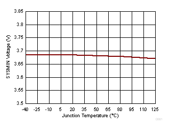
| VSYS_MIN |
System regulation voltage |
VVBAT < SYS_MIN[2:0] = 101, BATFET Disabled (REG07[5] = 1) |
3.5 |
3.68 |
|
V |
| VSYS |
System Regulation Voltage |
ISYS = 0 A, VVBAT > VSYSMIN, VVBAT = 4.400 V, BATFET disabled (REG07[5] = 1) |
|
VBAT + 50 mV |
|
V |
| VSYS_MAX |
Maximum DC system voltage output |
ISYS = 0 A, , Q4 off, VVBAT≤ 4.400 V, VVBAT > VSYSMIN = 3.5V |
4.4 |
4.45 |
4.48 |
V |
| RON(RBFET) |
Top reverse blocking MOSFET on-resistance between VBUS and PMID - Q1 |
-40°C≤ TA ≤ 125°C |
|
35 |
|
mΩ |
| RON(HSFET) |
Top switching MOSFET on-resistance between PMID and SW - Q2 |
VREGN = 5 V , -40°C≤ TA ≤ 125°C |
|
55 |
|
mΩ |
| RON(LSFET) |
Bottom switching MOSFET on-resistance between SW and GND - Q3 |
VREGN = 5 V , -40°C≤ TA ≤ 125°C |
|
60 |
|
mΩ |
| VFWD |
BATFET forward voltage in supplement mode |
|
|
30 |
|
mV |
| RON(BAT-SYS) |
SYS-BAT MOSFET on-resistance |
Measured from BAT to SYS, VBAT = 4.2V, TJ = –40 - 125°C |
|
19.5 |
|
mΩ |
| BATTERY CHARGER |
| VBATREG_RANGE |
Charge voltage program range |
|
3.856 |
|
4.624 |
V |
| VBATREG_STEP |
Charge voltage step |
|
|
32 |
|
mV |
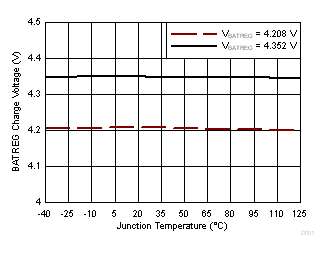
| VBATREG |
Charge voltage setting |
VREG (REG04[7:3]) = 4.208 V (01011), V, –40 ≤ TJ ≤ 85°C |
4.187 |
4.208 |
4.229 |
V |
| VREG (REG04[7:3]) = 4.352 V (01111), V, –40 ≤ TJ ≤ 85°C |
4.330 |
4.352 |
4.374 |
V |
| VBATREG_ACC |
Charge voltage setting accuracy |
VBAT = 4.208 V or VBAT = 4.352 V, –40 ≤ TJ ≤ 85°C |
–0.5% |
|
0.5% |
|
| ICHG_REG_RANGE |
Charge current regulation range |
|
0 |
|
3000 |
mA |
| ICHG_REG_STEP |
Charge current regulation step |
|
|
60 |
|
mA |
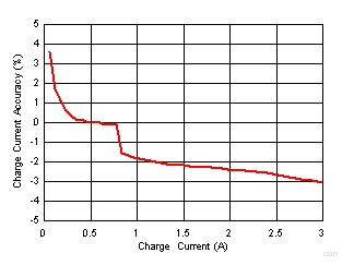
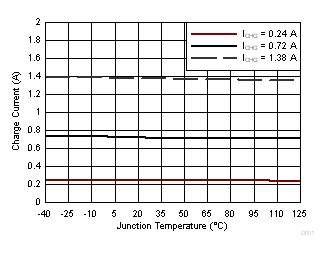
| ICHG_REG |
Charge current regulation setting |
ICHG = 240 mA, VVBAT = 3.1V or VVBAT = 3.8 V |
0.214 |
0.24 |
0.26 |
A |
| ICHG_REG_ACC |
Charge current regulation accuracy |
ICHG = 240 mA, VVBAT = 3.1 V or VVBAT = 3.8 V |
–11% |
|
9% |
|
| ICHG_REG |
Charge current regulation setting |
ICHG = 720 mA, VVBAT = 3.1 V or VVBAT = 3.8 V |
0.68 |
0.720 |
0.76 |
A |
| ICHG_REG |
Charge current regulation accuracy |
ICHG_REG = 720 mA, VBAT = 3.1 V or VBAT = 3.8 V |
-6% |
|
6% |
|
| ICHG_REG |
Charge current regulation setting |
ICHG = 1.38 A, VVBAT = 3.1 V or VVBAT = 3.8 V |
1.30 |
1.380 |
1.45 |
A |
| ICHG_REG_ACC |
Charge current regulation accuracy |
ICHG = 720 mA or ICHG = 1.38 A, VVBAT = 3.1 V or VVBAT = 3.8 V |
–6% |
|
6% |
|
| VBATLOWV_FALL |
Battery LOWV falling threshold |
ICHG = 240 mA |
2.7 |
2.8 |
2.9 |
V |
| VBATLOWV_RISE |
Battery LOWV rising threshold |
Pre-charge to fast charge |
3 |
3.12 |
3.24 |
V |
| IPRECHG |
Precharge current regulation |
IPRECHG[3:0] = '0010' = 180 mA |
150 |
170 |
190 |
mA |
| IPRECHG_ACC |
Precharge current regulation accuracy |
IPRECHG[3:0] = '0010' = 180 mA |
–15 |
|
5 |
% |
| ITERM |
Termination current regulation |
ICHG > 780 mA, ITERM[3:0] = '0010' = 180 mA, VVBAT = 4.208 V |
145 |
180 |
215 |
mA |
| ITERM_ACC |
Termination current regulation accuracy |
ICHG > 780 mA, , ITERM[3:0] = '0010' = 180 mA, VVBAT = 4.208 V |
-20% |
|
20% |
|
| ITERM |
Termination current regulation |
ICHG ≤ 780 mA, , ITERM[3:0] = '0000' = 60 mA, VVBAT = 4.208 V |
44 |
60 |
75 |
mA |
| ITERM_ACC |
Termination current regulation accuracy |
ICHG ≤ 780 mA, ,ITERM[3:0] = '0000' = 60 mA, VVBAT = 4.208 V |
-27% |
|
25% |
|
| VSHORT |
Battery short voltage |
VVBAT falling |
1.85 |
2 |
2.15 |
V |
| VSHORTZ |
Battery short voltage |
VVBAT rising |
2.15 |
2.25 |
2.35 |
V |
| ISHORT |
Battery short current |
VVBAT < VSHORTZ |
50 |
90 |
117 |
mA |
| VRECHG |
Recharge Threshold below VBAT_REG |
VBAT falling, REG04[0] = 0 |
90 |
120 |
150 |
mV |
| VRECHG |
Recharge Threshold below VBAT_REG |
VBAT falling, REG04[0] = 1 |
200 |
230 |
265 |
mV |
| ISYSLOAD |
System discharge load current |
VSYS = 4.2 V |
|
30 |
|
mA |
| INPUT VOLTAGE AND CURRENT REGULATION |
| VINDPM |
Input voltage regulation limit |
VINDPM (REG06[3:0] = 0000) = 3.9 V |
3.78 |
3.95 |
4.1 |
V |
| VINDPM_ACC |
Input voltage regulation accuracy |
VINDPM (REG06[3:0] = 0000) = 3.9 V |
–4.5% |
|
4% |
|
| VINDPM |
Input voltage regulation limit |
VINDPM (REG06[3:0] = 0110) = 4.4 V |
4.268 |
4.4 |
4.532 |
V |
| VINDPM_ACC |
Input voltage regulation accuracy |
VINDPM (REG06[3:0] = 0110) = 4.4 V |
–3% |
|
3% |
|
| VDPM_VBAT |
Input voltage regulation limit tracking VBAT |
VINDPM = 3.9V, VDPM_VBAT_TRACK = 300mV, VBAT = 4.0V |
4.17 |
4.3 |
4.46 |
V |
| VDPM_VBAT_ACC |
Input voltage regulation accuracy tracking VBAT |
VINDPM = 3.9V, VDPM_VBAT_TRACK = 300mV, VBAT = 4.0V |
–3% |
|
4% |
|
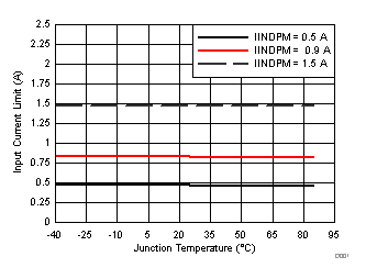
| IINDPM |
USB input current regulation limit |
VVBUS = 5 V, current pulled from SW, IINDPM (REG[4:0] = 00100) = 500 mA, –40 ≤ TJ ≤ 85°C |
450 |
|
500 |
mA |
| VVBUS = 5 V, current pulled from SW, IINDPM (REG[4:0] = 01000) = 900 mA, –40 ≤ TJ ≤ 85°C |
750 |
|
900 |
mA |
| VVBUS = 5 V, current pulled from SW, IINDPM (REG[4:0] = 01110) = 1.5 A, –40 ≤ TJ ≤ 85°C |
1.28 |
|
1.5 |
A |
| IIN_START |
Input current limit during system start-up sequence |
|
|
200 |
|
mA |
| BAT PIN OVERVOLTAGE PROTECTION |
| VBATOVP_RISE |
Battery overvoltage threshold |
VBAT rising, as percentage of VBAT_REG |
103 |
104 |
105 |
% |
| VBATOVP_Fall_HYS |
Battery overvoltage falling hysteresis |
VBAT falling, as percentage of VBAT_REG |
|
2 |
|
% |
| THERMAL REGULATION AND THERMAL SHUTDOWN |
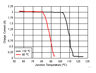
| TJUNCTION_REG |
Junction Temperature Regulation Threshold |
Temperature Increasing, TREG (REG05[1] = 1) = 110℃ |
|
110 |
|
°C |
| TJUNCTION_REG |
Junction Temperature Regulation Threshold |
Temperature Increasing, TREG (REG05[1] = 0) = 90℃ |
|
90 |
|
°C |
| TSHUT |
Thermal Shutdown Rising Temperature |
Temperature Increasing |
|
160 |
|
°C |
| TSHUT_HYST |
Thermal Shutdown Hysteresis |
|
|
30 |
|
°C |
| CHARGE OVERCURRENT COMPARATOR (CYCLE-BY-CYCLE) |
| IBATFET_OCP |
System over load threshold |
|
6.0 |
|
|
A |
| PWM |
| fSW |
PWM switching frequency |
Oscillator frequency, buck mode |
1320 |
1500 |
1680 |
kHz |
| DMAX |
Maximum PWM duty cycle(1) |
|
|
97% |
|
|
| REGN LDO |
| VREGN |
REGN LDO output voltage |
VVBUS = 9V, IREGN = 40mA |
5.6 |
6 |
6.65 |
V |
| VREGN |
REGN LDO output voltage |
VVBUS = 5V, IREGN = 20mA |
4.58 |
4.7 |
4.8 |
V |
| LOGIC I/O PIN CHARACTERISTICS (CE, PSEL, SCL, SDA,, INT) |
| VILO |
Input low threshold CE |
|
|
|
0.4 |
V |
| VIH |
Input high threshold CE |
|
1.3 |
|
|
V |
| IBIAS |
High-level leakage current CE |
Pull up rail 1.8 V |
|
|
1 |
µA |
| VILO |
Input low threshold PSEL |
|
|
|
0.4 |
V |
| VIH |
Input high threshold PSEL |
|
1.3 |
|
|
V |
| IBIAS |
High-level leakage current PSEL |
Pull up rail 1.8V |
|
|
1 |
µA |
| LOGIC I/O PIN CHARACTERISTICS (PG, STAT) |
| VOL |
Low-level output voltage |
|
|
|
0.4 |
V |
