SLUSD88A March   2019  – June 2019 BQ25886

PRODUCTION DATA.  

  1. Features
  2. Applications
  3. Description
    1.     Simplified Schematic
  4. Revision History
  5. Device Comparison Table
  6. Pin Configuration and Functions
    1.     Pin Functions
  7. Specifications
    1. 7.1 Absolute Maximum Ratings
    2. 7.2 ESD Ratings
    3. 7.3 Recommended Operating Conditions
    4. 7.4 Thermal Information
    5. 7.5 Electrical Characteristics
    6. 7.6 Timing Requirements
    7. 7.7 Typical Characteristics
  8. Detailed Description
    1. 8.1 Overview
    2. 8.2 Functional Block Diagram
    3. 8.3 Feature Description
      1. 8.3.1  Device Power-On-Reset
      2. 8.3.2  Device Power Up from Battery without Input Source
      3. 8.3.3  Device Power Up from Input Source
        1. 8.3.3.1 Poor Source Qualification
        2. 8.3.3.2 Input Source Type Detection
          1. 8.3.3.2.1 D+/D– Detection Sets Input Current Limit
        3. 8.3.3.3 Power Up REGN Regulator (LDO)
        4. 8.3.3.4 Converter Power Up
      4. 8.3.4  Input Current Optimizer (ICO)
      5. 8.3.5  Buck Mode Operation from Battery (OTG)
      6. 8.3.6  PowerPath Management
        1. 8.3.6.1 Narrow VDC Architecture
        2. 8.3.6.2 Dynamic Power Management
        3. 8.3.6.3 Supplement Mode
      7. 8.3.7  Battery Charging Management
        1. 8.3.7.1 Autonomous Charging Cycle
        2. 8.3.7.2 Battery Charging Profile
        3. 8.3.7.3 Charging Termination
        4. 8.3.7.4 Thermistor Qualification
          1. 8.3.7.4.1 JEITA Guideline Compliance in Charge Mode
        5. 8.3.7.5 Charging Safety Timer
      8. 8.3.8  Status Outputs
        1. 8.3.8.1 Power Good Indicator (PG)
        2. 8.3.8.2 Charging Status Indicator (STAT)
      9. 8.3.9  Input Current Limit on ILIM Pin
      10. 8.3.10 Voltage and Current Monitoring
        1. 8.3.10.1 Voltage and Current Monitoring in Boost Mode
          1. 8.3.10.1.1 Input Over-Voltage Protection
          2. 8.3.10.1.2 Input Under-Voltage Protection
          3. 8.3.10.1.3 System Over-Voltage Protection
          4. 8.3.10.1.4 System Over-Current Protection
        2. 8.3.10.2 Voltage and Current Monitoring in OTG Buck Mode
          1. 8.3.10.2.1 VBUS Over-voltage Protection
          2. 8.3.10.2.2 VBUS Over-Current Protection
      11. 8.3.11 Thermal Regulation and Thermal Shutdown
        1. 8.3.11.1 Thermal Protection in Boost Mode
        2. 8.3.11.2 Thermal Protection in OTG Buck Mode
      12. 8.3.12 Battery Protection
        1. 8.3.12.1 Battery Over-Voltage Protection (BATOVP)
    4. 8.4 Device Functional Modes
  9. Application and Implementation
    1. 9.1 Application Information
    2. 9.2 Typical Application
      1. 9.2.1 Design Requirements
      2. 9.2.2 Detailed Design Procedure
        1. 9.2.2.1 Inductor Selection
        2. 9.2.2.2 Input (VBUS / PMID) Capacitor
        3. 9.2.2.3 Output (VSYS) Capacitor
        4. 9.2.2.4 ILIM resistor
        5. 9.2.2.5 ICHGSET resistor
      3. 9.2.3 Application Curves
  10. 10Power Supply Recommendations
  11. 11Layout
    1. 11.1 Layout Guidelines
    2. 11.2 Layout Example
  12. 12Device and Documentation Support
    1. 12.1 Device Support
      1. 12.1.1 Third-Party Products Disclaimer
    2. 12.2 Documentation Support
      1. 12.2.1 Related Documentation
    3. 12.3 Receiving Notification of Documentation Updates
    4. 12.4 Community Resources
    5. 12.5 Trademarks
    6. 12.6 Electrostatic Discharge Caution
    7. 12.7 Glossary
  13. 13Mechanical, Packaging, and Orderable Information

Package Options

Mechanical Data (Package|Pins)
Thermal pad, mechanical data (Package|Pins)
Orderable Information

Application Curves

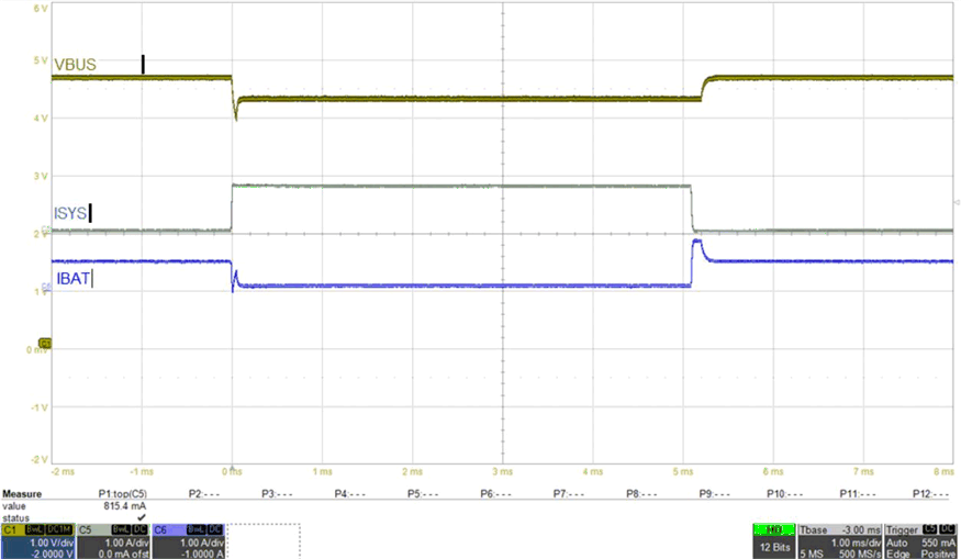
CVBUS = 1 µF, CPMID= 10 µF, CBAT = 10 µF, CSYS = 44 µF, L = DFE252012F-1R0 (1 µH) (unless otherwise specified)
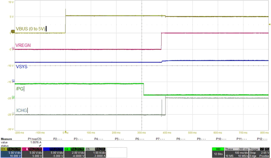
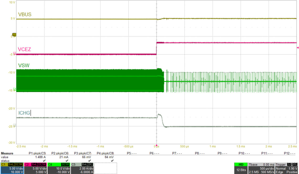
BQ25886 881_Adapter-Power-Up-with-Charge-Enabled.gif
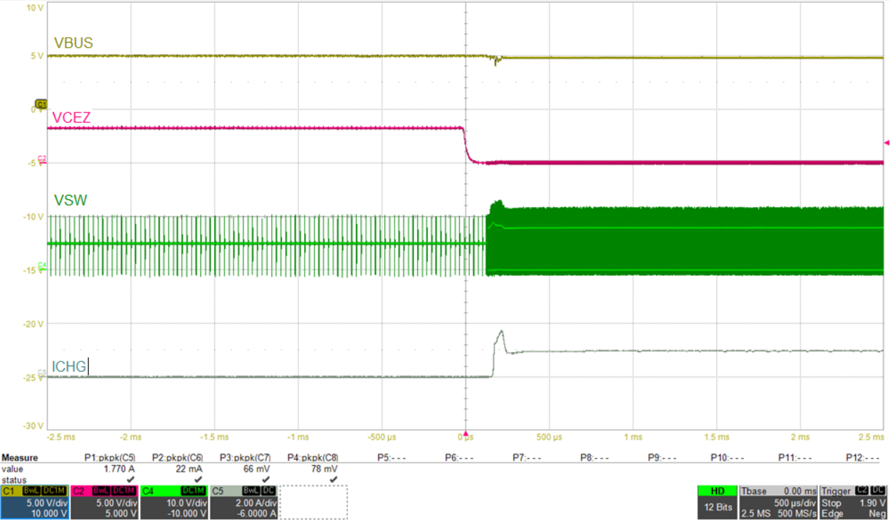
VBUS = 5 V VBAT = 6.0 V ICHG = 1 A
Figure 21. Adapter Power Up with Charge Enabled
BQ25886 886_Charge-Disable.png
VBUS = 5 V VBAT = 7.4 V ICHG = 1 A
Figure 23. Charge Disabled
BQ25886 886_Buck-Mode-(OTG)-Startup.png
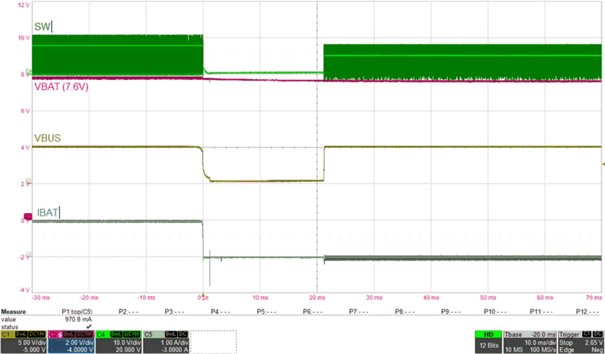
VBAT = 7.6 V VBUS = 5.1 V No IBUS load
Figure 25. Buck Mode (OTG) Startup
BQ25886 881_Buck-Mode-(OTG)-PWM-Switching.gif
VBAT = 7.6 V VBUS = 5.1 V IBUS = 1 A
Figure 27. Buck Mode (OTG) PWM Switching
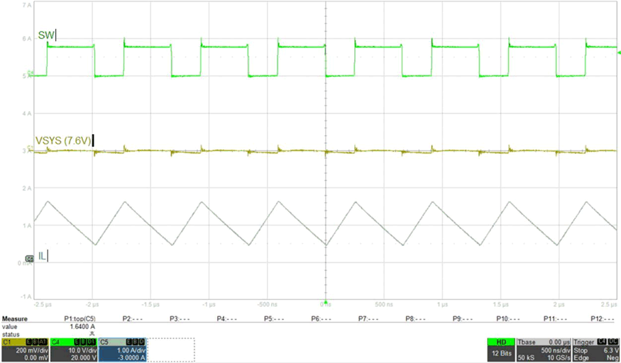
BQ25886 881_Boost-Mode-PWM-Switching.gif
VBUS = 5 V VBAT = 7.6 V ICHG = 1 A
Figure 29. Boost Mode PWM Switching
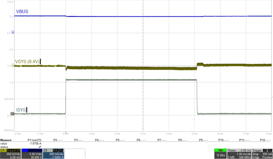
BQ25886 881_System-Load-Transient-Response.gif
VBUS = 5 V VBAT = 8.4 V Charge disabled
Figure 31. System Load Transient Response
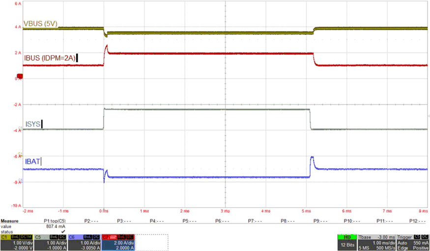
BQ25886 881_IINDPM-Transient-Response.gif
DCP Adapter VBAT = 8.0 V Charge enabled
Figure 33. IINDPM Transient Response
BQ25886 886_Charge-Enable.png
VBUS = 5 V VBAT = 7.4 V ICHG = 1 A
Figure 22. Charge Enable
BQ25886 881_Adapter-Plug-in-with-No-Battery.gif
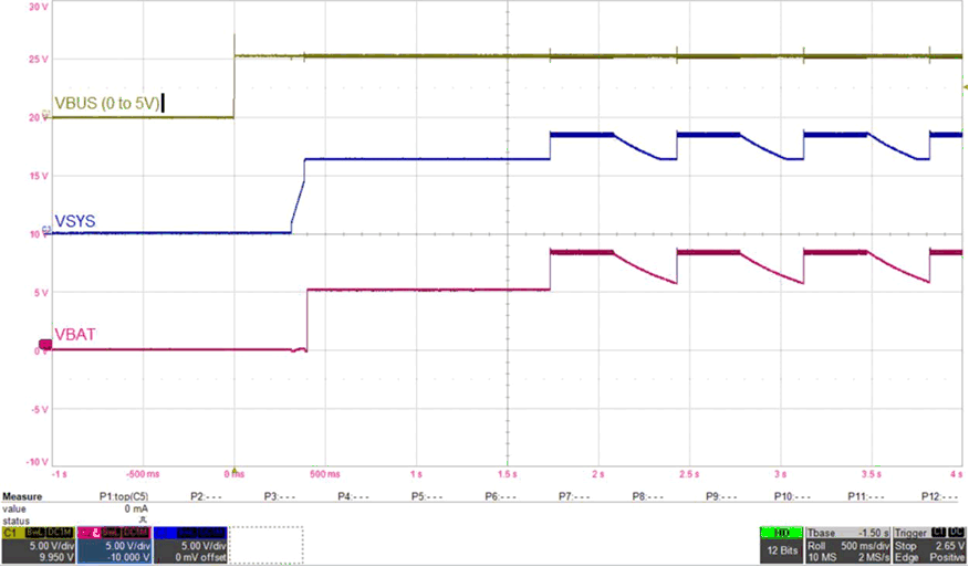
VBUS = 5 V VBAT = Open Charge enabled
Figure 24. Adapter Plug-in with No Battery
BQ25886 881_Buck-Mode-Startup-After-Adapter-Removal.gif
VBAT = 7.6 V Adapter removed with OTG = HIGH RBUS = 25 Ω
Figure 26. Buck Mode Startup After Adapter Removal
BQ25886 881_Buck-Mode-(OTG)-PFM-Switching.gif
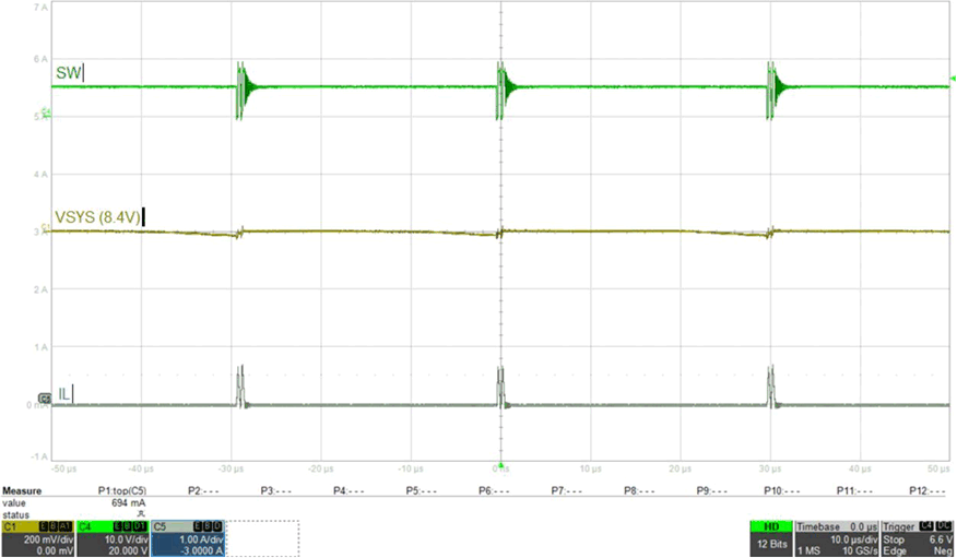
VBAT = 7.6 V VBUS = 5.1 V IBUS = 0 mA
Figure 28. Buck Mode (OTG) PFM Switching
BQ25886 881_Boost-Mode-PFM-Switching.gif
VBUS = 5 V VBAT = 8.4 V Charge disabled
Figure 30. Boost Mode PFM Switching
BQ25886 881_VINDPM-Transient-Response.gif
DCP Adapter VBAT = 8.0 V Charge enabled
Figure 32. VINDPM Transient Response
BQ25886 881_Buck-Mode-(OTG)-Load-Transient-Resposne.gif
VBAT = 7.6 V VBUS = 5.1 V
Figure 34. Buck Mode (OTG) Load Transient Response