SLUSD88A March   2019  – June 2019 BQ25886

PRODUCTION DATA.  

  1. Features
  2. Applications
  3. Description
    1.     Simplified Schematic
  4. Revision History
  5. Device Comparison Table
  6. Pin Configuration and Functions
    1.     Pin Functions
  7. Specifications
    1. 7.1 Absolute Maximum Ratings
    2. 7.2 ESD Ratings
    3. 7.3 Recommended Operating Conditions
    4. 7.4 Thermal Information
    5. 7.5 Electrical Characteristics
    6. 7.6 Timing Requirements
    7. 7.7 Typical Characteristics
  8. Detailed Description
    1. 8.1 Overview
    2. 8.2 Functional Block Diagram
    3. 8.3 Feature Description
      1. 8.3.1  Device Power-On-Reset
      2. 8.3.2  Device Power Up from Battery without Input Source
      3. 8.3.3  Device Power Up from Input Source
        1. 8.3.3.1 Poor Source Qualification
        2. 8.3.3.2 Input Source Type Detection
          1. 8.3.3.2.1 D+/D– Detection Sets Input Current Limit
        3. 8.3.3.3 Power Up REGN Regulator (LDO)
        4. 8.3.3.4 Converter Power Up
      4. 8.3.4  Input Current Optimizer (ICO)
      5. 8.3.5  Buck Mode Operation from Battery (OTG)
      6. 8.3.6  PowerPath Management
        1. 8.3.6.1 Narrow VDC Architecture
        2. 8.3.6.2 Dynamic Power Management
        3. 8.3.6.3 Supplement Mode
      7. 8.3.7  Battery Charging Management
        1. 8.3.7.1 Autonomous Charging Cycle
        2. 8.3.7.2 Battery Charging Profile
        3. 8.3.7.3 Charging Termination
        4. 8.3.7.4 Thermistor Qualification
          1. 8.3.7.4.1 JEITA Guideline Compliance in Charge Mode
        5. 8.3.7.5 Charging Safety Timer
      8. 8.3.8  Status Outputs
        1. 8.3.8.1 Power Good Indicator (PG)
        2. 8.3.8.2 Charging Status Indicator (STAT)
      9. 8.3.9  Input Current Limit on ILIM Pin
      10. 8.3.10 Voltage and Current Monitoring
        1. 8.3.10.1 Voltage and Current Monitoring in Boost Mode
          1. 8.3.10.1.1 Input Over-Voltage Protection
          2. 8.3.10.1.2 Input Under-Voltage Protection
          3. 8.3.10.1.3 System Over-Voltage Protection
          4. 8.3.10.1.4 System Over-Current Protection
        2. 8.3.10.2 Voltage and Current Monitoring in OTG Buck Mode
          1. 8.3.10.2.1 VBUS Over-voltage Protection
          2. 8.3.10.2.2 VBUS Over-Current Protection
      11. 8.3.11 Thermal Regulation and Thermal Shutdown
        1. 8.3.11.1 Thermal Protection in Boost Mode
        2. 8.3.11.2 Thermal Protection in OTG Buck Mode
      12. 8.3.12 Battery Protection
        1. 8.3.12.1 Battery Over-Voltage Protection (BATOVP)
    4. 8.4 Device Functional Modes
  9. Application and Implementation
    1. 9.1 Application Information
    2. 9.2 Typical Application
      1. 9.2.1 Design Requirements
      2. 9.2.2 Detailed Design Procedure
        1. 9.2.2.1 Inductor Selection
        2. 9.2.2.2 Input (VBUS / PMID) Capacitor
        3. 9.2.2.3 Output (VSYS) Capacitor
        4. 9.2.2.4 ILIM resistor
        5. 9.2.2.5 ICHGSET resistor
      3. 9.2.3 Application Curves
  10. 10Power Supply Recommendations
  11. 11Layout
    1. 11.1 Layout Guidelines
    2. 11.2 Layout Example
  12. 12Device and Documentation Support
    1. 12.1 Device Support
      1. 12.1.1 Third-Party Products Disclaimer
    2. 12.2 Documentation Support
      1. 12.2.1 Related Documentation
    3. 12.3 Receiving Notification of Documentation Updates
    4. 12.4 Community Resources
    5. 12.5 Trademarks
    6. 12.6 Electrostatic Discharge Caution
    7. 12.7 Glossary
  13. 13Mechanical, Packaging, and Orderable Information

Package Options

Mechanical Data (Package|Pins)
Thermal pad, mechanical data (Package|Pins)
Orderable Information

D+/D– Detection Sets Input Current Limit

The BQ25886 contains a D+/D- based input source detection to program the input current limit. The D+/D- detection has three major steps: Data Contact Detect (DCD), Primary Detection, and Secondary Detection.
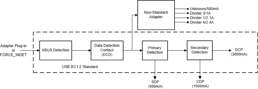
BQ25886 SLUSD64_dplus_dminus_detection_flow.gifFigure 13. D+/D- Detection Flow

Table 2. Non-Standard Adapter Detection

NON-STANDARD ADAPTER D+ THRESHOLD D– THRESHOLD INPUT CURRENT LIMIT
Divider 1 VD+ within V2P8_VTH VD– within V2P0_VTH 2.1 A
Divider 3 VD+ within V2P0_VTH VD– within V2P8_VTH 1 A
Divider 4 VD+ within V2P8_VTH VD– within V2P8_VTH 2.4 A

Table 3. Input Current Limit Setting from D+/D– Detection

D+/D– DETECTION INPUT CURRENT LIMIT (IINDPM)
USB SDP (USB500) 500 mA
USB CDP 1.5 A
USB DCP 3.0 A
Divider 3 1 A
Divider 1 2.1 A
Divider 4 2.4 A
Unknown 5V Adapter 500 mA