SLUSBF2C July 2013 – August 2015
PRODUCTION DATA.
- 1 Features
- 2 Applications
- 3 Description
- 4 Revision History
- 5 Device Comparison Table
- 6 Pin Configuration and Functions
-
7 Specifications
- 7.1 Absolute Maximum Ratings
- 7.2 ESD Ratings
- 7.3 Recommended Operating Conditions
- 7.4 Thermal Information
- 7.5 Power-On Reset
- 7.6 2.5-V LDO Regulator
- 7.7 Charger Attachment and Removal Detection
- 7.8 Voltage Doubler
- 7.9 Overvoltage Protection (OVP)
- 7.10 Undervoltage Protection (UVP)
- 7.11 Overcurrent in Discharge (OCD)
- 7.12 Overcurrent in Charge (OCC)
- 7.13 Short-Circuit in Discharge (SCD)
- 7.14 Low-Voltage Charging
- 7.15 Internal Temperature Sensor Characteristics
- 7.16 Internal Clock Oscillators
- 7.17 Integrating ADC (Coulomb Counter) Characteristics
- 7.18 ADC (Temperature and Cell Voltage) Characteristics
- 7.19 Data Flash Memory Characteristics
- 7.20 I2C-Compatible Interface Timing Characteristics
- 7.21 HDQ Communication Timing Characteristics
- 7.22 Typical Characteristics
-
8 Detailed Description
- 8.1 Overview
- 8.2 Functional Block Diagram
- 8.3 Feature Description
- 8.4
Device Functional Modes
- 8.4.1 NORMAL Mode
- 8.4.2 SLEEP Mode
- 8.4.3 FULLSLEEP Mode
- 8.4.4
Battery Protector Description
- 8.4.4.1 High-Side N-Channel FET Charge and Discharge FET Drive
- 8.4.4.2
Operating Modes
- 8.4.4.2.1 VIRTUAL SHUTDOWN Mode
- 8.4.4.2.2 UNDERVOLTAGE FAULT Mode
- 8.4.4.2.3 NORMAL Mode
- 8.4.4.2.4 SHUTDOWN WAIT Mode
- 8.4.4.2.5 OVERCURRENT IN DISCHARGE (OCD) and SHORT-CIRCUIT IN DISCHARGE (SCD) FAULT Mode
- 8.4.4.2.6 OVERCURRENT IN CHARGE (OCC) FAULT Mode
- 8.4.4.2.7 OVERVOLTAGE PROTECTION (OVP) FAULT Mode
- 8.4.4.3 Firmware Control of Protector
- 8.4.5 OVERTEMPERATURE FAULT Mode
-
9 Application and Implementation
- 9.1 Application Information
- 9.2
Typical Applications
- 9.2.1
Pack-Side, Single-Cell Li-Ion Fuel Gauge and Protector
- 9.2.1.1 Design Requirements
- 9.2.1.2
Detailed Design Procedure
- 9.2.1.2.1 BAT Voltage Sense Input
- 9.2.1.2.2 SRP and SRN Current Sense Inputs
- 9.2.1.2.3 Sense Resistor Selection
- 9.2.1.2.4 TS Temperature Sense Input
- 9.2.1.2.5 Thermistor Selection
- 9.2.1.2.6 VPWR Power Supply Input Filtering
- 9.2.1.2.7 REG25 LDO Output Filtering
- 9.2.1.2.8 Communication Interface Lines
- 9.2.1.2.9 PACKP Voltage Sense Input
- 9.2.1.2.10 CHG and DSG Charge Pump Voltage Outputs
- 9.2.1.2.11 N-Channel FET Selection
- 9.2.1.2.12 Additional ESD Protection Components
- 9.2.1.3 Application Curves
- 9.2.1
Pack-Side, Single-Cell Li-Ion Fuel Gauge and Protector
- 10Power Supply Recommendations
- 11Layout
- 12Device and Documentation Support
- 13Mechanical, Packaging, and Orderable Information
Package Options
Mechanical Data (Package|Pins)
- YZF|15
Thermal pad, mechanical data (Package|Pins)
Orderable Information
9 Application and Implementation
NOTE
Information in the following applications sections is not part of the TI component specification, and TI does not warrant its accuracy or completeness. TI’s customers are responsible for determining suitability of components for their purposes. Customers should validate and test their design implementation to confirm system functionality.
9.1 Application Information
The bq27741-G1 device is a single-cell fuel gauge with integrated Li-Ion protection circuitry for highly accurate detection of overvoltage, undervoltage, overcurrent in charge, overcurrent in discharge, and short-circuit in discharge fault conditions. If the detected fault continues to be present for a specific delay time (pre-configured in the device), the protection front-end will disable the applicable charge pump circuit, resulting in opening of the FET until the provoking safety condition resolves. The integrated 16-bit delta-sigma converters provide accurate, high precision measurements for voltage, current, and temperature in order to accomplish effective battery monitoring, protection, and gauging. To allow for optimal performance in the end application, special considerations must be taken to ensure minimization of measurement error through proper printed circuit board (PCB) layout and correct configuration of battery characteristics in the fuel gauge data flash. Such requirements are detailed in Design Requirements.
9.2 Typical Applications
9.2.1 Pack-Side, Single-Cell Li-Ion Fuel Gauge and Protector
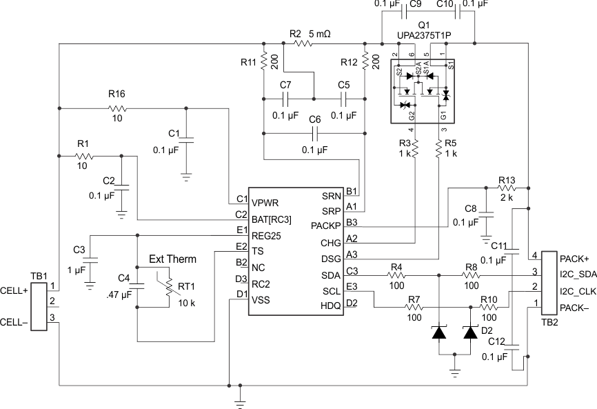 Figure 11. Typical Application Schematic, I2C Mode
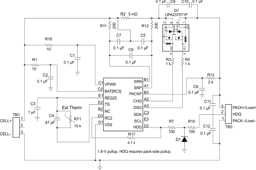 Figure 12. Typical Application Schematic, HDQ Mode
9.2.1.1 Design Requirements
Several key parameters must be updated to align with a given application's battery characteristics. For highest accuracy gauging, it is important to follow-up this initial configuration with a learning cycle to optimize resistance and maximum chemical capacity (Qmax) values prior to sealing and shipping packs to the field. Successful and accurate configuration of the fuel gauge for a target application can be used as the basis for creating a "golden" file that can be written to all production packs, assuming identical pack design and Li-Ion cell origin (chemistry, lot, and so on). Calibration data can be included as part of this golden file to cut down on battery pack production time. If using this method, it is recommended to average the calibration data from a large sample size and use these in the golden file.
NOTE
It is recommended to calibrate all packs individually as this will lead to the highest performance and lowest measurement error in the end application on a per-pack basis. In addition, the integrated protection functionality should be correctly configured to ensure activation based on the fault protection needs of the target pack design, or else accidental trip could be possible if using defaults.
Table 3 shows the items that should be configured to achieve reliable protection and accurate gauging with minimal initial configuration.
Table 3. Key Data Flash Parameters for Configuration
| NAME | DEFAULT | UNIT | RECOMMENDED SETTING |
|---|---|---|---|
| Design Capacity | 1000 | mAh | Set based on the nominal pack capacity as shown in the cell manufacturer's data sheet. If multiple parallel cells are used, should be set to N × Cell Capacity. |
| Design Energy | 3800 | mWh | Set based on the nominal pack energy (nominal cell voltage × nominal cell capacity) as shown in the cell manufacturer's data sheet. If multiple parallel cells are used, should be set to N × Cell Energy. |
| Design Energy Scale | 1 | — | Set to 10 to convert all power values to cWh or to 1 for mWh. Design Energy is divided by this value. |
| Reserve Capacity | 0 | mAh | Set to desired runtime remaining (in seconds/3600) × typical applied load between reporting 0% SOC and reaching Terminate Voltage, if needed. |
| Design Voltage | 3800 | mV | Set to nominal cell voltage per manufacturer data sheet. |
| Cycle Count Threshold | 900 | mAh | Set to 90% of configured Design Capacity. |
| Device Chemistry | 0354 | hex | Should be configured using TI-supplied Battery Management Studio (bqStudio) software. Default open-circuit voltage and resistance tables are also updated in conjunction with this step. Do not attempt to manually update reported Device Chemistry as this does not change all chemistry information. Always update chemistry using the appropriate software tool (that is, bqStudio). |
| Load Mode | 1 | — | Set to applicable load model, 0 for constant current or 1 for constant power. |
| Load Select | 1 | — | Set to load profile which most closely matches typical system load. |
| Qmax Cell 0 | 1000 | mAh | Set to initial configured value for Design Capacity. The gauge will update this parameter automatically after the optimization cycle and for every regular Qmax update thereafter. |
| V at Chg Term | 4350 | mV | Set to nominal cell voltage for a fully charged cell. The gauge will update this parameter automatically each time full charge termination is detected. |
| Terminate Voltage | 3000 | mV | Set to empty point reference of battery based on system needs. Typical is between 3000 and 3200 mV. |
| Ra Max Delta | 43 | mΩ | Set to 15% of Cell0 R_a 4 resistance after an optimization cycle is completed. |
| Charging Voltage | 4350 | mV | Set based on nominal charge voltage for the battery in normal conditions (25°C, and so on). Used as the reference point for offsetting by Taper Voltage for full charge termination detection. |
| Taper Current | 100 | mA | Set to the nominal taper current of the charger + taper current tolerance to ensure that the gauge will reliably detect charge termination. |
| Taper Voltage | 100 | mV | Sets the voltage window for qualifying full charge termination. Can be set tighter to avoid or wider to ensure possibility of reporting 100% SOC in outer JEITA temperature ranges that use derated charging voltage. |
| Dsg Current Threshold | 60 | mA | Sets threshold for gauge detecting battery discharge. Should be set lower than minimal system load expected in the application and higher than Quit Current. |
| Chg Current Threshold | 75 | mA | Sets the threshold for detecting battery charge. Can be set higher or lower depending on typical trickle charge current used. Also should be set higher than Quit Current. |
| Quit Current | 40 | mA | Sets threshold for gauge detecting battery relaxation. Can be set higher or lower depending on typical standby current and exhibited in the end system. |
| Avg I Last Run | –299 | mA | Current profile used in capacity simulations at onset of discharge or at all times if Load Select = 0. Should be set to nominal system load. Is automatically updated by the gauge every cycle. |
| Avg P Last Run | –1131 | mW | Power profile used in capacity simulations at onset of discharge or at all times if Load Select = 0. Should be set to nominal system power. Is automatically updated by the gauge every cycle. |
| Sleep Current | 15 | mA | Sets the threshold at which the fuel gauge enters SLEEP mode. Take care in setting above typical standby currents else entry to SLEEP may be unintentionally blocked. |
| Shutdown V | 0 | mV | If auto-shutdown of fuel gauge is required prior to protect against accidental discharge to undervoltage condition, set this to desired voltage threshold for completely powering down the fuel gauge. Recovery occurs when a charger is connected. |
| OT Chg | 55 | °C | Set to desired temperature at which charging is prohibited to prevent cell damage due to excessive ambient temperature. |
| OT Chg Time | 5 | s | Set to desired time before CHG FET is disabled based on overtemperature. Since temperature changes much more slowly than other fault conditions, the default setting is sufficient for most application. |
| OT Chg Recovery | 50 | °C | Set to the temperature threshold at which charging is no longer prohibited. |
| OT Dsg | 60 | °C | Set to desired temperature at which discharging is prohibited to prevent cell damage due to excessive ambient temperature. |
| OT Dsg Time | 5 | s | Set to desired time before DSG FET is disabled based on overtemperature. Since temperature changes much more slowly than other fault conditions, the default setting is sufficient for most application. |
| OT Dsg Recovery | 55 | °C | Set to the temperature threshold at which cell discharging is no longer prohibited. |
| CC Gain | 5 | mΩ | Calibrate this parameter using TI-supplied bqStudio software and calibration procedure in the TRM. Determines conversion of coulomb counter measured sense resistor voltage to current. |
| CC Delta | 5.074 | mΩ | Calibrate this parameter using TI-supplied bqStudio software and calibration procedure in the TRM. Determines conversion of coulomb counter measured sense resistor voltage to passed charge. |
| CC Offset | 6.874 | mA | Calibrate this parameter using TI-supplied bqStudio software and calibration procedure in the TRM. Determines native offset of coulomb counter hardware that should be removed from conversions. |
| Board Offset | 0.66 | µA | Calibrate this parameter using TI-supplied bqStudio software and calibration procedure in the TRM. Determines native offset of the printed circuit board parasitics that should be removed from conversions. |
| Pack V Offset | 0 | mV | Calibrate this parameter using TI-supplied bqStudio software and calibration procedure in the TRM. Determines voltage offset between cell tab and ADC input node to incorporate back into or remove from measurement, depending on polarity. |
9.2.1.2 Detailed Design Procedure
9.2.1.2.1 BAT Voltage Sense Input
A ceramic capacitor at the input to the BAT pin is used to bypass AC voltage ripple to ground, greatly reducing its influence on battery voltage measurements. It is most effective in applications with load profiles that exhibit high frequency current pulses (that is, cell phones), but is recommended for use in all applications to reduce noise on this sensitive high impedance measurement node.
The series resistor between the battery and the BAT input is used to limit current that could be conducted through the chip-scale package's solder bumps in the event of an accidental short during the board assembly process. The resistor is not likely to survive a sustained short condition (depends on power rating); however, it damages the much cheaper resistor component over suffering damage to the fuel gauge die itself.
9.2.1.2.2 SRP and SRN Current Sense Inputs
The filter network at the input to the coulomb counter is intended to improve differential mode rejection of voltage measured across the sense resistor. These components should be placed as close as possible to the coulomb counter inputs and the routing of the differential traces length-matched in order to best minimize impedance mismatch-induced measurement errors. The single-ended ceramic capacitors should be tied to the battery voltage node (preferably to a large copper pour connected to the SRN side of the sense resistor) in order to further improve common-mode noise rejection. The series resistors between the CC inputs and the sense resistor should be at least 200 Ω in order to mitigate SCR-induced latch-up due to possible ESD events.
9.2.1.2.3 Sense Resistor Selection
Any variation encountered in the resistance present between the SRP and SRN pins of the fuel gauge will affect the resulting differential voltage and derived current it senses. As such, it is recommended to select a sense resistor with minimal tolerance and temperature coefficient of resistance (TCR) characteristics. The standard recommendation based on best compromise between performance and price is a 1% tolerance, 50-ppm drift sense resistor with a 1-W power rating.
9.2.1.2.4 TS Temperature Sense Input
Similar to the BAT pin, a ceramic decoupling capacitor for the TS pin is used to bypass AC voltage ripple away from the high-impedance ADC input, minimizing measurement error. Another helpful advantage is that the capacitor provides additional ESD protection since most thermistors are handled and manually soldered to the PCB as a separate step in the factory production flow. It should be placed as close as possible to the respective input pin for optimal filtering performance.
9.2.1.2.5 Thermistor Selection
The fuel gauge temperature sensing circuitry is designed to work with a negative temperature coefficient-type (NTC) thermistor with a characteristic 10-kΩ resistance at room temperature (25°C). The default curve-fitting coefficients configured in the fuel gauge specifically assume a 103AT-2 type thermistor profile and so that is the default recommendation for thermistor selection purposes. Moving to a separate thermistor resistance profile (for example, JT-2 or others) requires an update to the default thermistor coefficients in data flash to ensure highest accuracy temperature measurement performance.
9.2.1.2.6 VPWR Power Supply Input Filtering
A ceramic capacitor is placed at the input to the fuel gauge's internal LDO in order to increase power supply rejection (PSR) and improve effective line regulation. It ensures that voltage ripple is rejected to ground instead of coupling into the device's internal supply rails.
9.2.1.2.7 REG25 LDO Output Filtering
A ceramic capacitor is also needed at the output of the internal LDO to provide a current reservoir for fuel gauge load peaks during high peripheral utilization. It acts to stabilize the regulator output and reduce core voltage ripple inside of the device.
9.2.1.2.8 Communication Interface Lines
A protection network composed of resistors and zener diodes is recommended on each of the serial communication inputs to protect the fuel gauge from serious ESD transients. The Zener should be selected to break down at a voltage larger than the typical pullup voltage for these lines but less than the internal diode clamp breakdown voltage of the device inputs (approximately 6 V). A zener voltage of 5.6 V is typically recommended. The series resistors are used to limit the current into the Zener diode and prevent component destruction due to thermal strain once it goes into breakdown. 100 Ω is typically recommended for these resistance values.
9.2.1.2.9 PACKP Voltage Sense Input
Inclusion of a 2-kΩ series resistor on the PACKP input allows it to tolerate a charger overvoltage event up to 28 V without device damage. The resistor also protects the device in the event of a reverse polarity charger input, since the substrate diode will be forward biased and attempt to conduct charger current through the fuel gauge (as well as the high FETs). An external reverse charger input FET clamp can be added to short the DSG FET gate to its source terminal, forcing the conduction channel off when negative voltage is present at PACK+ input to the battery pack and preventing large battery discharge currents. A ceramic capacitor connected at the PACKP pin helps to filter voltage into the comparator sense lines used for checking charger and load presence. In addition, in the LOW VOLTAGE CHARGING state, the minimal circuit elements that are operational are powered from this input pin and require a stable supply.
9.2.1.2.10 CHG and DSG Charge Pump Voltage Outputs
The series resistors used at the DSG and CHG output pins serve to protect them from damaging ESD events or breakdown conditions, allowing the resistors to be damaged in place of the fuel gauge itself. An added bonus is that they also help to limit in-rush currents due to use of FETs with large gate capacitance, allowing a smooth ramp of power-path connection turn-on to the system.
9.2.1.2.11 N-Channel FET Selection
The selection of N-channel FETs for a single-cell battery pack design depends on a variety of factors including package type, size, and device cost as well as performance metrics such as drain-to-source resistance (rDS(on)), gate capacitance, maximum current and power handling, and similar. At a minimum, it is recommended that the selected FETs have a drain-to-source voltage (VDS) and gate-to-source (VGS) voltage tolerance of 12 V. Some FETs are designed to handle as much as 24 V between the drain and source terminals and this would provide an increased safety margin for the pack design. Additionally, the DC current rating should be high enough to safely handle sustained current in charge or discharge direction just below the maximum threshold tolerances of the configured OCC and OCD protections and the lowest possible sense resistance value based on tolerance and TCR considerations, or vice-versa. This ensures that there is sufficient power dissipation margin given a worst-case scenario for the fault detections. In addition, striving for minimal FET resistance at the expected gate bias as well as lowest gate capacitance will help reduce conduction losses and increase power efficiency as well as achieve faster turn-on and turn-off times for the FETs. Many of these FETs are now offered as dual, back-to-back N-channel FETs in wafer-chip scale (WCSP) packaging, decreasing both BOM count and shrinking necessary board real estate to accommodate the components. Finally, refer to the safe operating area (SOA) curves of the target FETs to ensure that the boundaries are never violated based on all possible load conditions in the end application. The CSD83325L is an excellent example of a FET solution that meets all of the aforementioned criteria, offering rDS(on) of 10.3 mΩ and VDS of 12 V with back-to-back N-channel FETs in a chip-scale package, a perfect fit for battery pack designs.
9.2.1.2.12 Additional ESD Protection Components
The additional capacitors placed across the CHG and DSF FET source pins as well as between PACK+ and ground help to bolster and greatly improve the ESD robustness of the pack design. The former components shunt damaging transients around the FETs and the latter components attempt to bypass such pulses to PACK– before they couple further into the battery pack PCB. Two series capacitors are used for each of these protection areas to prevent a battery short in the event of a single capacitor failure.
9.2.1.3 Application Curves
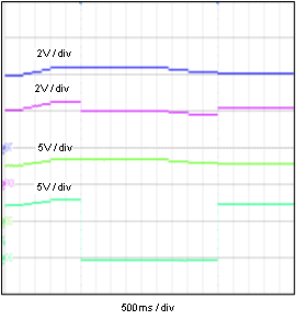 Figure 13. Overvoltage Protection Set and Clear
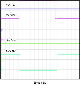 Figure 15. Overcurrent in Charge Protection Set and Clear
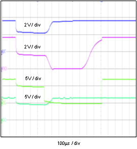 Figure 17. Short-Circuit in Discharge Protection Set and Clear
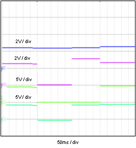 Figure 14. Undervoltage Protection Set and Clear
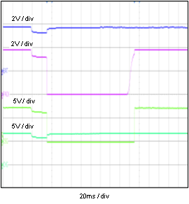 Figure 16. Overcurrent in Discharge Protection Set and Clear