SLUSBF2C July 2013 – August 2015
PRODUCTION DATA.
- 1 Features
- 2 Applications
- 3 Description
- 4 Revision History
- 5 Device Comparison Table
- 6 Pin Configuration and Functions
-
7 Specifications
- 7.1 Absolute Maximum Ratings
- 7.2 ESD Ratings
- 7.3 Recommended Operating Conditions
- 7.4 Thermal Information
- 7.5 Power-On Reset
- 7.6 2.5-V LDO Regulator
- 7.7 Charger Attachment and Removal Detection
- 7.8 Voltage Doubler
- 7.9 Overvoltage Protection (OVP)
- 7.10 Undervoltage Protection (UVP)
- 7.11 Overcurrent in Discharge (OCD)
- 7.12 Overcurrent in Charge (OCC)
- 7.13 Short-Circuit in Discharge (SCD)
- 7.14 Low-Voltage Charging
- 7.15 Internal Temperature Sensor Characteristics
- 7.16 Internal Clock Oscillators
- 7.17 Integrating ADC (Coulomb Counter) Characteristics
- 7.18 ADC (Temperature and Cell Voltage) Characteristics
- 7.19 Data Flash Memory Characteristics
- 7.20 I2C-Compatible Interface Timing Characteristics
- 7.21 HDQ Communication Timing Characteristics
- 7.22 Typical Characteristics
-
8 Detailed Description
- 8.1 Overview
- 8.2 Functional Block Diagram
- 8.3 Feature Description
- 8.4
Device Functional Modes
- 8.4.1 NORMAL Mode
- 8.4.2 SLEEP Mode
- 8.4.3 FULLSLEEP Mode
- 8.4.4
Battery Protector Description
- 8.4.4.1 High-Side N-Channel FET Charge and Discharge FET Drive
- 8.4.4.2
Operating Modes
- 8.4.4.2.1 VIRTUAL SHUTDOWN Mode
- 8.4.4.2.2 UNDERVOLTAGE FAULT Mode
- 8.4.4.2.3 NORMAL Mode
- 8.4.4.2.4 SHUTDOWN WAIT Mode
- 8.4.4.2.5 OVERCURRENT IN DISCHARGE (OCD) and SHORT-CIRCUIT IN DISCHARGE (SCD) FAULT Mode
- 8.4.4.2.6 OVERCURRENT IN CHARGE (OCC) FAULT Mode
- 8.4.4.2.7 OVERVOLTAGE PROTECTION (OVP) FAULT Mode
- 8.4.4.3 Firmware Control of Protector
- 8.4.5 OVERTEMPERATURE FAULT Mode
-
9 Application and Implementation
- 9.1 Application Information
- 9.2
Typical Applications
- 9.2.1
Pack-Side, Single-Cell Li-Ion Fuel Gauge and Protector
- 9.2.1.1 Design Requirements
- 9.2.1.2
Detailed Design Procedure
- 9.2.1.2.1 BAT Voltage Sense Input
- 9.2.1.2.2 SRP and SRN Current Sense Inputs
- 9.2.1.2.3 Sense Resistor Selection
- 9.2.1.2.4 TS Temperature Sense Input
- 9.2.1.2.5 Thermistor Selection
- 9.2.1.2.6 VPWR Power Supply Input Filtering
- 9.2.1.2.7 REG25 LDO Output Filtering
- 9.2.1.2.8 Communication Interface Lines
- 9.2.1.2.9 PACKP Voltage Sense Input
- 9.2.1.2.10 CHG and DSG Charge Pump Voltage Outputs
- 9.2.1.2.11 N-Channel FET Selection
- 9.2.1.2.12 Additional ESD Protection Components
- 9.2.1.3 Application Curves
- 9.2.1
Pack-Side, Single-Cell Li-Ion Fuel Gauge and Protector
- 10Power Supply Recommendations
- 11Layout
- 12Device and Documentation Support
- 13Mechanical, Packaging, and Orderable Information
Package Options
Mechanical Data (Package|Pins)
- YZF|15
Thermal pad, mechanical data (Package|Pins)
Orderable Information
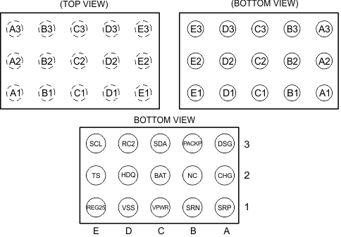
6 Pin Configuration and Functions
Pin Functions
| PIN | I/O(1) | DESCRIPTION | |
|---|---|---|---|
| NAME | NO. | ||
| BAT | C2 | IA | Cell-voltage measurement input. ADC input |
| CHG | A2 | O | External high-side N-channel charge FET driver |
| DSG | A3 | O | External high-side N-channel discharge FET driver |
| HDQ | D2 | IO | HDQ serial communications line. Open-drain |
| PACKP | B3 | IA | Pack voltage measurement input for protector operation |
| NC | B2 | IO | Not used. Reserved for future GPIO. Recommended to connect to GND. |
| RC2 | D3 | IO | General purpose IO. Push-pull output |
| REG25 | E1 | P | Regulator output and bq27741-G1 processor power. Decouple with 1-µF ceramic capacitor to VSS. |
| SCL | E3 | IO | Slave I2C serial communications clock input line for communication with system. Use with 10-kΩ pullup resistor (typical). |
| SDA | C3 | IO | Slave I2C serial communications data line for communication with system. Open-drain I/O. Use with 10-kΩ pullup resistor (typical). |
| SRN | B1 | IA | Analog input pin connected to the internal coulomb counter where SRN is nearest the CELL+ connection. Connect to sense resistor. |
| SRP | A1 | IA | Analog input pin connected to the internal coulomb counter where SRP is nearest the PACK+ connection. Connect to sense resistor. |
| VPWR | C1 | P | Power input. Decouple with 0.1-µF ceramic capacitor to VSS. |
| VSS | D1 | P | Device ground |
| TS | E2 | IA | Pack thermistor voltage sense (use 103AT-type thermistor). ADC input |
(1) IO = Digital input-output, IA = Analog input, P = Power connection, O = Output
Table 1. Default Configuration
| OVERVOLTAGE PROTECTION (VOVP) | UNDERVOLTAGE PROTECTION (VUVP) | OVERCURRENT IN DISCHARGE (VOCD) | OVERCURRENT IN CHARGE (VOCC) | SHORT CIRCUIT IN DISCHARGE (Vscd) |
|---|---|---|---|---|
| 4.390 V | 2.407 V | 34.4 mV | 20 mV | 74.6 mV |
| OVERVOLTAGE PROTECTION DELAY (tOVP) | UNDERVOLTAGE PROTECTION DELAY (tUVP) | OVERCURRENT IN DISCHARGE DELAY (tOCD) | OVERCURRENT IN CHARGE DELAY (tOCC) | SHORT CIRCUIT IN DISCHARGE DELAY (tscd) |
|---|---|---|---|---|
| 1 s | 31.25 ms | 31.25 ms | 7.8125 ms | 312.5 µs |
