SLUSBF2C July 2013 – August 2015
PRODUCTION DATA.
- 1 Features
- 2 Applications
- 3 Description
- 4 Revision History
- 5 Device Comparison Table
- 6 Pin Configuration and Functions
-
7 Specifications
- 7.1 Absolute Maximum Ratings
- 7.2 ESD Ratings
- 7.3 Recommended Operating Conditions
- 7.4 Thermal Information
- 7.5 Power-On Reset
- 7.6 2.5-V LDO Regulator
- 7.7 Charger Attachment and Removal Detection
- 7.8 Voltage Doubler
- 7.9 Overvoltage Protection (OVP)
- 7.10 Undervoltage Protection (UVP)
- 7.11 Overcurrent in Discharge (OCD)
- 7.12 Overcurrent in Charge (OCC)
- 7.13 Short-Circuit in Discharge (SCD)
- 7.14 Low-Voltage Charging
- 7.15 Internal Temperature Sensor Characteristics
- 7.16 Internal Clock Oscillators
- 7.17 Integrating ADC (Coulomb Counter) Characteristics
- 7.18 ADC (Temperature and Cell Voltage) Characteristics
- 7.19 Data Flash Memory Characteristics
- 7.20 I2C-Compatible Interface Timing Characteristics
- 7.21 HDQ Communication Timing Characteristics
- 7.22 Typical Characteristics
-
8 Detailed Description
- 8.1 Overview
- 8.2 Functional Block Diagram
- 8.3 Feature Description
- 8.4
Device Functional Modes
- 8.4.1 NORMAL Mode
- 8.4.2 SLEEP Mode
- 8.4.3 FULLSLEEP Mode
- 8.4.4
Battery Protector Description
- 8.4.4.1 High-Side N-Channel FET Charge and Discharge FET Drive
- 8.4.4.2
Operating Modes
- 8.4.4.2.1 VIRTUAL SHUTDOWN Mode
- 8.4.4.2.2 UNDERVOLTAGE FAULT Mode
- 8.4.4.2.3 NORMAL Mode
- 8.4.4.2.4 SHUTDOWN WAIT Mode
- 8.4.4.2.5 OVERCURRENT IN DISCHARGE (OCD) and SHORT-CIRCUIT IN DISCHARGE (SCD) FAULT Mode
- 8.4.4.2.6 OVERCURRENT IN CHARGE (OCC) FAULT Mode
- 8.4.4.2.7 OVERVOLTAGE PROTECTION (OVP) FAULT Mode
- 8.4.4.3 Firmware Control of Protector
- 8.4.5 OVERTEMPERATURE FAULT Mode
-
9 Application and Implementation
- 9.1 Application Information
- 9.2
Typical Applications
- 9.2.1
Pack-Side, Single-Cell Li-Ion Fuel Gauge and Protector
- 9.2.1.1 Design Requirements
- 9.2.1.2
Detailed Design Procedure
- 9.2.1.2.1 BAT Voltage Sense Input
- 9.2.1.2.2 SRP and SRN Current Sense Inputs
- 9.2.1.2.3 Sense Resistor Selection
- 9.2.1.2.4 TS Temperature Sense Input
- 9.2.1.2.5 Thermistor Selection
- 9.2.1.2.6 VPWR Power Supply Input Filtering
- 9.2.1.2.7 REG25 LDO Output Filtering
- 9.2.1.2.8 Communication Interface Lines
- 9.2.1.2.9 PACKP Voltage Sense Input
- 9.2.1.2.10 CHG and DSG Charge Pump Voltage Outputs
- 9.2.1.2.11 N-Channel FET Selection
- 9.2.1.2.12 Additional ESD Protection Components
- 9.2.1.3 Application Curves
- 9.2.1
Pack-Side, Single-Cell Li-Ion Fuel Gauge and Protector
- 10Power Supply Recommendations
- 11Layout
- 12Device and Documentation Support
- 13Mechanical, Packaging, and Orderable Information
Package Options
Mechanical Data (Package|Pins)
- YZF|15
Thermal pad, mechanical data (Package|Pins)
Orderable Information
7 Specifications
7.1 Absolute Maximum Ratings
over operating free-air temperature range (unless otherwise noted)(1)| MIN | MAX | UNIT | ||
|---|---|---|---|---|
| VVPWR | Power input | –0.3 | 5.5 | V |
| VREG25 | Supply voltage | –0.3 | 2.75 | V |
| VPACKP | PACKP input pin | –0.3 | 5.5 | V |
| PACK+ input when external 2-kΩ resistor is in series with PACKP input pin (see (1)) | –0.3 | 28 | V | |
| VOUT | Voltage output pins (DSG, CHG) | –0.3 | 10 | V |
| VIOD1 | Push-pull IO pins (RC2) | –0.3 | 2.75 | V |
| VIOD2 | Open-drain IO pins (SDA, SCL, HDQ, NC) | –0.3 | 5.5 | V |
| VBAT | BAT input pin | –0.3 | 5.5 | V |
| VI | Input voltage to all other pins (SRP, SRN) | –0.3 | 5.5 | V |
| VTS | Input voltage for TS | –0.3 | 2.75 | V |
| TA | Operating free-air temperature | –40 | 85 | °C |
| TF | Functional temperature | –40 | 100 | °C |
| TSTG | Storage temperature | –65 | 150 | °C |
(1) Stresses beyond those listed under Absolute Maximum Ratings may cause permanent damage to the device. These are stress ratings only, which do not imply functional operation of the device at these or any other conditions beyond those indicated under Recommended Operating Conditions. Exposure to absolute-maximum-rated conditions for extended periods may affect device reliability.
7.2 ESD Ratings
| VALUE | UNIT | |||
|---|---|---|---|---|
| V(ESD) | Electrostatic discharge | Human-body model (HBM), per ANSI/ESDA/JEDEC JS-001(1) | ±2000 | V |
| Charged-device model (CDM), per JEDEC specification JESD22-C101(2) | ±500 | |||
(1) JEDEC document JEP155 states that 500-V HBM allows safe manufacturing with a standard ESD control process.
(2) JEDEC document JEP157 states that 250-V CDM allows safe manufacturing with a standard ESD control process.
7.3 Recommended Operating Conditions
TA = 25°C, CREG25 = 1.0 µF, and VVPWR = 3.6 V (unless otherwise noted)| PARAMETER | TEST CONDITION | MIN | NOM | MAX | UNIT | |
|---|---|---|---|---|---|---|
| VVPWR | Supply voltage | No operating restrictions | 2.8 | 5 | V | |
| No FLASH writes | 2.45 | 2.8 | ||||
| CVPWR | External input capacitor for internal LDO between VPWR and VSS | Nominal capacitor values specified. Recommend a 5% ceramic X5R type capacitor located close to the device. | 0.1 | µF | ||
| CREG25 | External output capacitor for internal LDO between REG25 and VSS | 0.47 | 1 | µF | ||
| ICC | Normal operating mode current(1)(2) (VPWR) | Fuel gauge in NORMAL mode. ILOAD > Sleep Current with charge pumps on (FETs on) |
167 | µA | ||
| ISLP | SLEEP mode current(1)(2) (VPWR) | Fuel gauge in SLEEP+ mode. ILOAD < Sleep Current with charge pumps on (FETs on) |
88 | µA | ||
| IFULLSLP | FULLSLEEP mode current(1)(2) (VPWR) | Fuel gauge in SLEEP mode. ILOAD < Sleep Current with charge pumps on (FETs on) |
40 | µA | ||
| ISHUTDOWN | Shutdown mode current(1)(2) (VPWR) | Fuel gauge in SHUTDOWN mode. UVP tripped with fuel gauge and protector turned off (FETs off) VVPWR = 2.5 V TA = 25°C |
0.1 | 0.2 | µA | |
| TA = –40°C to 85°C | 0.5 | µA | ||||
| VOL | Output voltage low (SCL, SDA, HDQ, NC, RC2) | IOL = 1 mA | 0.4 | V | ||
| VOH(OD) | Output voltage high (SDA, SCL, HDQ, NC, RC2) | External pullup resistor connected to VREG25 | VREG25 – 0.5 | V | ||
| VIL | Input voltage low (SDA, SCL, HDQ, NC) | –0.3 | 0.6 | V | ||
| VIH(OD) | Input voltage high (SDA, SCL, HDQ, NC) | 1.2 | 5.5 | V | ||
| VA1 | Input voltage range (TS) | VSS – 0.125 | 2 | V | ||
| VA2 | Input voltage range (BAT) | VSS – 0.125 | 5 | V | ||
| VA3 | Input voltage range (SRP, SRN) | VVPWR – 0.125 | VVPWR + 0.125 | V | ||
| Ilkg | Input leakage current (I/O pins) | 0.3 | µA | |||
| tPUCD | Power-up communication delay | 250 | ms | |||
(1) All currents are specified as charge pump on (FETs on).
(2) All currents are continuous average over 5-second period.
7.4 Thermal Information
| THERMAL METRIC(1) | bq27741-G1 | UNIT | |
|---|---|---|---|
| YZF [DSBGA] | |||
| 15 PINS | |||
| RθJA | Junction-to-ambient thermal resistance | 70 | °C/W |
| RθJC(top) | Junction-to-case (top) thermal resistance | 17 | |
| RθJB | Junction-to-board thermal resistance | 20 | |
| ψJT | Junction-to-top characterization parameter | 1 | |
| ψJB | Junction-to-board characterization parameter | 18 | |
| RθJC(bot) | Junction-to-case (bottom) thermal resistance | N/A | |
(1) For more information about traditional and new thermal metrics, see the IC Package Thermal Metrics application report, SPRA953.
7.5 Power-On Reset
TA = 25°C, CREG25 = 1.0 µF, and VVPWR = 3.6 V (unless otherwise noted)| PARAMETER | TEST CONDITIONS | MIN | TYP | MAX | UNIT | |
|---|---|---|---|---|---|---|
| VIT+ | Increasing battery voltage input at VREG25 | 2.09 | 2.20 | 2.31 | V | |
| VHYS | Power-on reset hysteresis | 115 | mV | |||
7.6 2.5-V LDO Regulator(1)
TA = 25°C, CREG25 = 1.0 µF, and VVPWR = 3.6 V (unless otherwise noted)| PARAMETER | TEST CONDITIONS | MIN | TYP | MAX | UNIT | ||
|---|---|---|---|---|---|---|---|
| VREG25 | Regulator output voltage | 2.8 V ≤ VVPWR ≤ 4.5 V, IOUT(1) ≤ 16 mA |
TA = –40°C to 85°C | 2.3 | 2.5 | 2.6 | V |
| 2.45 V ≤ VVPWR < 2.8 V (low battery), IOUT(1) ≤ 3 mA |
2.3 | V | |||||
| ISHORT(2) | Short-circuit current limit | VREG25 = 0 V | TA = –40°C to 85°C | 250 | mA | ||
(1) LDO output current, IOUT, is the sum of internal and external load currents.
(2) Assured by characterization. Not production tested.
7.7 Charger Attachment and Removal Detection
TA = 25°C, CREG25 = 1.0 µF, and VVPWR = 3.6 V (unless otherwise noted)| PARAMETER | TEST CONDITIONS | MIN | TYP | MAX | UNIT | |
|---|---|---|---|---|---|---|
| VCHGATT | Voltage threshold for charger attachment detection | 2.7 | 3 | V | ||
| VCHGREM | Voltage threshold for charger removal detection | 0.5 | 1 | V | ||
7.8 Voltage Doubler
TA = 25°C, CREG25 = 1.0 µF, and VVPWR = 3.6 V (unless otherwise noted)| PARAMETER | TEST CONDITIONS | MIN | TYP | MAX | UNIT | |
|---|---|---|---|---|---|---|
| VFETON | CHG and DSG FETs on | IL = 1 µA TA = –40°C to 85°C |
2 × VVPWR – 0.4 | 2 × VVPWR – 0.2 | 2 × VVPWR | V |
| VFETOFF | CHG and DSG FETs off | TA = –40°C to 85°C | 0.2 | V | ||
| VFETRIPPLE(1) | CHG and DSG FETs on | IL = 1 µA TA = –40°C to 85°C |
0.1 | VPP | ||
| tFETON | FET gate rise time (10% to 90%) |
CL = 4 nF TA = –40°C to 85°C No series resistance |
67 | 140 | 218 | μs |
| tFETOFF | FET gate fall time (90% to 10%) |
CL = 4 nF TA = –40°C to 85°C No series resistance |
10 | 30 | 60 | μs |
(1) Assured by characterization. Not production tested.
7.9 Overvoltage Protection (OVP)
TA = 25°C and CREG25 = 1.0 µF (unless otherwise noted)| PARAMETER | TEST CONDITIONS | MIN | TYP | MAX | UNIT | |
|---|---|---|---|---|---|---|
| VOVP | OVP detection voltage threshold | TA = 25°C | VOVP – 0.006 | VOVP | VOVP + 0.006 | V |
| TA = 0°C to 25°C | VOVP – 0.023 | VOVP | VOVP + 0.020 | |||
| TA = 25°C to 50°C | VOVP – 0.018 | VOVP | VOVP + 0.014 | |||
| TA = –40°C to 85°C | VOVP – 0.053 | VOVP | VOVP + 0.035 | |||
| VOVPREL | OVP release voltage | TA = 25°C | VOVPREL – 0.012 | VOVP – 0.215 | VOVPREL + 0.012 | V |
| TA = 0°C to 25°C | VOVPREL – 0.023 | VOVP – 0.215 | VOVPREL + 0.020 | |||
| TA = 25°C to 50°C | VOVPREL – 0.018 | VOVP – 0.215 | VOVPREL + 0.014 | |||
| TA = –40°C to 85°C | VOVPREL – 0.053 | VOVP – 0.215 | VOVPREL + 0.035 | |||
| tOVP | OVP delay time | TA = –40°C to 85°C | tOVP – 5% | tOVP | tOVP + 5% | s |
7.10 Undervoltage Protection (UVP)
TA = 25°C and CREG25 = 1.0 µF (unless otherwise noted)| PARAMETER | TEST CONDITIONS | MIN | TYP | MAX | UNIT | |
|---|---|---|---|---|---|---|
| VUVP | UVP detection voltage threshold | TA = 25°C | VUVP – 0.012 | VUVP | VUVP + 0.012 | V |
| TA = –5°C to 50°C | VUVP – 0.020 | VUVP | VUVP + 0.020 | |||
| TA = –40°C to 85°C | VUVP – 0.040 | VUVP | VUVP + 0.040 | |||
| VUVPREL | UVP release voltage | TA = 25°C | VUVPREL – 0.012 | VUVP + 0.105 | VUVPREL + 0.012 | V |
| TA = –5°C to 50°C | VUVPREL – 0.020 | VUVP + 0.105 | VUVPREL + 0.020 | |||
| TA = –40°C to 85°C | VUVPREL – 0.040 | VUVP + 0.105 | VUVPREL + 0.040 | |||
| tUVP | UVP delay time | TA = –40°C to 85°C | tUVP – 5% | tUVP | tUVP + 5% | ms |
7.11 Overcurrent in Discharge (OCD)
TA = 25°C, CREG25 = 1.0 µF, and VVPWR = 3.6 V (unless otherwise noted)| PARAMETER | TEST CONDITIONS | MIN | TYP | MAX | UNIT | |
|---|---|---|---|---|---|---|
| VOCD | OCD detection voltage threshold | TA = 25°C VSRN – VSRP |
VOCD – 3 | VOCD | VOCD + 3 | mV |
| TA = –20°C to 60°C VSRN – VSRP |
VOCD – 3.785 | VOCD | VOCD + 3.785 | |||
| TA = –40°C to 85°C VSRN – VSRP |
VOCD – 4.16 | VOCD | VOCD + 4.16 | |||
| tOCD | OCD delay time | TA = –40°C to 85°C | tOCD – 5% | tOCD | tOCD + 5% | ms |
7.12 Overcurrent in Charge (OCC)
TA = 25°C, CREG25 = 1.0 µF, and VVPWR = 3.6 V (unless otherwise noted)| PARAMETER | TEST CONDITIONS | MIN | TYP | MAX | UNIT | |
|---|---|---|---|---|---|---|
| VOCC | OCC detection voltage threshold | TA = 25°C VSRP – VSRN |
VOCC – 3 | VOCC | VOCC + 3 | mV |
| TA = –20°C to 60°C VSRP – VSRN |
VOCC – 3.49 | VOCC | VOCC + 3.49 | |||
| TA = –40°C to 85°C VSRP – VSRN |
VOCC – 3.86 | VOCC | VOCC + 3.86 | |||
| tOCC | OCC delay time | TA = –40°C to 85°C | tOCC – 5% | tOCC | tOCC + 5% | ms |
7.13 Short-Circuit in Discharge (SCD)
TA = 25°C, CREG25 = 1.0 µF, and VVPWR = 3.6 V (unless otherwise noted)| PARAMETER | TEST CONDITIONS | MIN | TYP | MAX | UNIT | |
|---|---|---|---|---|---|---|
| VSCD | SCD detection voltage threshold | TA = 25°C VSRN – VSRP |
VSCD – 3 | VSCD | VSCD + 3 | mV |
| TA = –20°C to 60°C VSRN – VSRP |
VSCD – 4.5 | VSCD | VSCD + 4.5 | |||
| TA = –40°C to 85°C VSRN – VSRP |
VSCD – 4.9 | VSCD | VSCD + 4.9 | |||
| tSCD | SCD delay time | TA = –40°C to 85°C | tSCD – 10% | tSCD | tSCD + 10% | µs |
7.14 Low-Voltage Charging
TA = 25°C, CREG25 = 1.0 µF, and VVPWR = 3.6 V (unless otherwise noted)| PARAMETER | TEST CONDITIONS | MIN | TYP | MAX | UNIT | |
|---|---|---|---|---|---|---|
| VLVDET | Voltage threshold for low-voltage charging detection | TA = –40°C to 85°C | 1.4 | 1.55 | 1.7 | V |
7.15 Internal Temperature Sensor Characteristics
TA = –40°C to 85°C, 2.4 V < VREG25 < 2.6 V| PARAMETER | TEST CONDITIONS | MIN | TYP | MAX | UNIT | |
|---|---|---|---|---|---|---|
| G(TEMP) | Temperature sensor voltage gain | –2 | mV/°C | |||
7.16 Internal Clock Oscillators
2.4 V < VREG25 < 2.6 V; typical values at TA = 25°C and VREG25 = 2.5 V (unless otherwise noted)| PARAMETER | TEST CONDITIONS | MIN | TYP | MAX | UNIT | |
|---|---|---|---|---|---|---|
| fOSC | Operating frequency | 8.389 | MHz | |||
| f(LOSC) | Operating frequency | 32.768 | kHz | |||
7.17 Integrating ADC (Coulomb Counter) Characteristics
TA = –40°C to 85°C, 2.4 V < VREG25 < 2.6 V; typical values at TA = 25°C and VREG25 = 2.5 V (unless otherwise noted)| PARAMETER | TEST CONDITIONS | MIN | TYP | MAX | UNIT | |
|---|---|---|---|---|---|---|
| VSR_IN | Input voltage range, VSRN and VSRP | VSR = VSRN – VSRP | VVPWR – 0.125 | VVPWR + 0.125 | V | |
| tSR_CONV | Conversion time | Single conversion | 1 | s | ||
| Resolution | 14 | 15 | bits | |||
| VSR_OS | Input offset | 10 | μV | |||
| INL | Integral nonlinearity error | ±0.007% | ±0.034% | FSR | ||
| ZSR_IN | Effective input resistance(1) | 7 | MΩ | |||
| ISR_LKG | Input leakage current(1) | 0.3 | μA | |||
(1) Assured by design. Not production tested.
7.18 ADC (Temperature and Cell Voltage) Characteristics
TA = –40°C to 85°C, 2.4 V < VREG25 < 2.6 V; typical values at TA = 25°C and VREG25 = 2.5 V (unless otherwise noted)| PARAMETER | TEST CONDITIONS | MIN | TYP | MAX | UNIT | |
|---|---|---|---|---|---|---|
| VADC_IN | Input voltage range (VBAT channel) | VSS – 0.125 | 5 | V | ||
| Input voltage range (other channels) | VSS – 0.125 | 1 | V | |||
| tADC_CONV | Conversion time | 125 | ms | |||
| Resolution | 14 | 15 | bits | |||
| VADC_OS | Input offset | 1 | mV | |||
| ZADC1 | Effective input resistance (TS) (1) | 55 | MΩ | |||
| ZADC2 | Effective input resistance (BAT)(1) | Not measuring cell voltage | 55 | MΩ | ||
| Measuring cell voltage | 100 | kΩ | ||||
| IADC_LKG | Input leakage current(1) | 0.3 | μA | |||
(1) Assured by design. Not production tested.
7.19 Data Flash Memory Characteristics
TA = –40°C to 85°C, 2.4 V < VREG25 < 2.6 V; typical values at TA = 25°C and VREG25 = 2.5 V (unless otherwise noted)| PARAMETER | TEST CONDITIONS | MIN | TYP | MAX | UNIT | |
|---|---|---|---|---|---|---|
| tDR | Data retention(1) | 10 | years | |||
| Flash programming write-cycles (1) | 20,000 | cycles | ||||
| tWORDPROG | Word programming time(1) | 2 | ms | |||
| ICCPROG | Flash-write supply current(1) | 5 | 10 | mA | ||
(1) Assured by design. Not production tested.
7.20 I2C-Compatible Interface Timing Characteristics
TA = –40°C to 85°C, 2.4 V < VREG25 < 2.6 V; typical values at TA = 25°C and VREG25 = 2.5 V (unless otherwise noted)| MIN | TYP | MAX | UNIT | ||
|---|---|---|---|---|---|
| tR | SCL or SDA rise time | 300 | ns | ||
| tF | SCL or SDA fall time | 300 | ns | ||
| tw(H) | SCL pulse width (high) | 600 | ns | ||
| tw(L) | SCL pulse width (low) | 1.3 | μs | ||
| tsu(STA) | Setup for repeated start | 600 | ns | ||
| td(STA) | Start to first falling edge of SCL | 600 | ns | ||
| tsu(DAT) | Data setup time | 100 | ns | ||
| th(DAT) | Data hold time | 0 | ns | ||
| tsu(STOP) | Setup time for stop | 600 | ns | ||
| tBUF | Bus free time between stop and start | 66 | μs | ||
| fSCL | Clock frequency | 400 | kHz | ||
7.21 HDQ Communication Timing Characteristics
TA = –40°C to 85°C, 2.4 V < VREG25 < 2.6 V; typical values at TA = 25°C and VREG25 = 2.5 V (unless otherwise noted)| MIN | TYP | MAX | UNIT | ||
|---|---|---|---|---|---|
| t(CYCH) | Cycle time, host to fuel gauge | 190 | μs | ||
| t(CYCD) | Cycle time, fuel gauge to host | 190 | 205 | 250 | μs |
| t(HW1) | Host sends 1 to fuel gauge | 0.5 | 50 | μs | |
| t(DW1) | Fuel gauge sends 1 to host | 32 | 50 | μs | |
| t(HW0) | Host sends 0 to fuel gauge | 86 | 145 | μs | |
| t(DW0) | Fuel gauge sends 0 to host | 80 | 145 | μs | |
| t(RSPS) | Response time, fuel gauge to host | 190 | 950 | μs | |
| t(B) | Break time | 190 | μs | ||
| t(BR) | Break recovery time | 40 | μs | ||
| t(RST) | HDQ reset | 1.8 | 2.2 | s | |
| t(RISE) | HDQ line rise time to logic 1 (1.2 V) | 950 | ns | ||
| t(TRND) | Turnaround time (time from the falling edge of the last transmitted bit of 8-bit data and the falling edge of the next Break signal) | 210 | μs | ||
 Figure 1. I2C-Compatible Interface Timing Diagrams
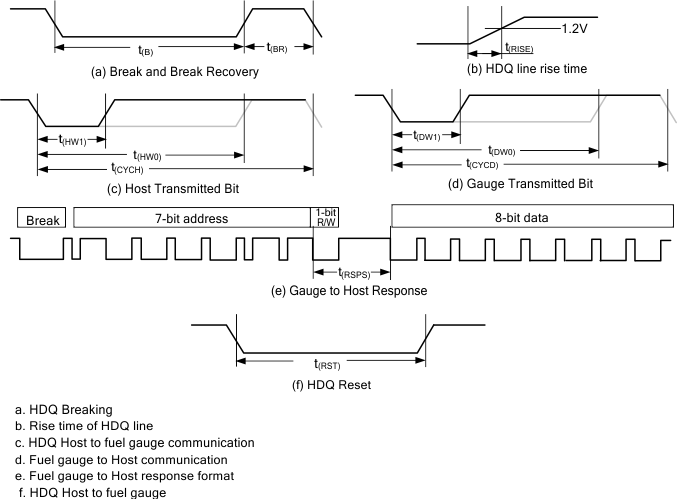 Figure 2. HDQ Timing Diagrams
7.22 Typical Characteristics
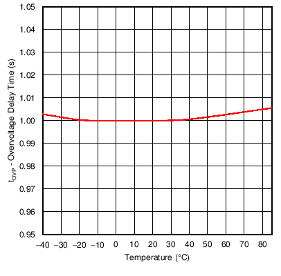 Figure 3. Overvoltage Delay Time
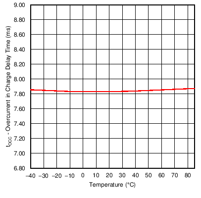 Figure 5. Overcurrent in Charge Delay Time
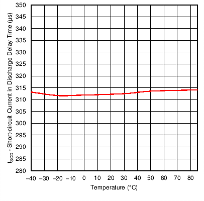 Figure 7. Short-Circuit Current in Discharge Delay Time
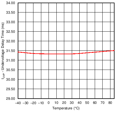 Figure 4. Undervoltage Delay Time
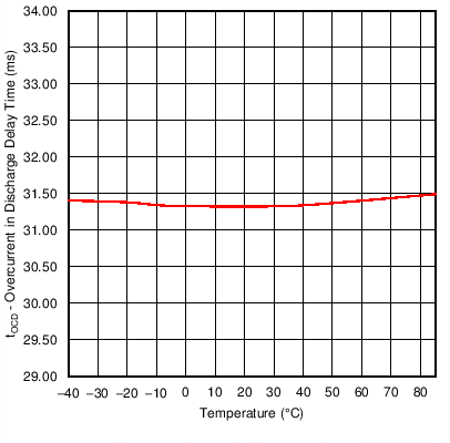 Figure 6. Overcurrent in Discharge Delay Time