SWRS045F January 2006 – November 2018 CC1021
PRODUCTION DATA.
- 1Device Overview
- 2Revision History
- 3Terminal Configuration and Functions
-
4Specifications
- 4.1 Absolute Maximum Ratings
- 4.2 ESD Ratings
- 4.3 Recommended Operating Conditions
- 4.4 RF Transmit
- 4.5 RF Receive
- 4.6 RSSI / Carrier Sense
- 4.7 Intermediate Frequency (IF)
- 4.8 Crystal Oscillator
- 4.9 Frequency Synthesizer
- 4.10 Digital Inputs / Outputs
- 4.11 Current Consumption
- 4.12 Thermal Resistance Characteristics for VQFNP Package
-
5Detailed Description
- 5.1 Overview
- 5.2 Functional Block Diagram
- 5.3 Configuration Overview
- 5.4 Microcontroller Interface
- 5.5 4-wire Serial Configuration Interface
- 5.6 Signal Interface
- 5.7 Data Rate Programming
- 5.8 Frequency Programming
- 5.9
Receiver
- 5.9.1 IF Frequency
- 5.9.2 Receiver Channel Filter Bandwidth
- 5.9.3 Demodulator, Bit Synchronizer and Data Decision
- 5.9.4 Receiver Sensitivity versus Data Rate and Frequency Separation
- 5.9.5 RSSI
- 5.9.6 Image Rejection Calibration
- 5.9.7 Blocking and Selectivity
- 5.9.8 Linear IF Chain and AGC Settings
- 5.9.9 AGC Settling
- 5.9.10 Preamble Length and Sync Word
- 5.9.11 Carrier Sense
- 5.9.12 Automatic Power-Up Sequencing
- 5.9.13 Automatic Frequency Control
- 5.9.14 Digital FM
- 5.10 Transmitter
- 5.11 Input and Output Matching and Filtering
- 5.12 Frequency Synthesizer
- 5.13 VCO and LNA Current Control
- 5.14 Power Management
- 5.15 On-Off Keying (OOK)
- 5.16 Crystal Oscillator
- 5.17 Built-in Test Pattern Generator
- 5.18 Interrupt on Pin DCLK
- 5.19 PA_EN and LNA_EN Digital Output Pins
- 5.20 System Considerations and Guidelines
- 5.21 Antenna Considerations
- 5.22 Configuration Registers
- 6Applications, Implementation, and Layout
- 7Device and Documentation Support
- 8Mechanical Packaging and Orderable Information
Package Options
Mechanical Data (Package|Pins)
- RSS|32
Thermal pad, mechanical data (Package|Pins)
- RSS|32
Orderable Information
5.12.2 VCO and PLL Self-Calibration
To compensate for supply voltage, temperature and process variations, the VCO and PLL must be calibrated. The calibration is performed automatically and sets the maximum VCO tuning range and optimum charge pump current for PLL stability. After setting up the device at the operating frequency, the self-calibration can be initiated by setting the CAL_START bit in the CALIBRATE register. The calibration result is stored internally in the chip, and is valid as long as power is not turned off. If large supply voltage drops (typically more than 0.25 V) or temperature variations (typically more than 40°C) occur after calibration, a new calibration should be performed.
The nominal VCO control voltage is set by the CAL_ITERATE[2:0] bits in the CALIBRATE register.
The CAL_COMPLETE bit in the STATUS register indicates that calibration has finished. The calibration wait time (CAL_WAIT) is programmable and is proportional to the internal PLL reference frequency. The highest possible reference frequency should be used to get the minimum calibration time. It is recommended to use CAL_WAIT[1:0] = 11 in order to get the most accurate loop bandwidth.
Table 5-11 Typical Calibration Times
| CALIBRATION TIME [MS] | REFERENCE FREQUENCY [MHz] | ||
|---|---|---|---|
| CAL_WAIT | 1.8432 | 7.3728 | 9.8304 |
| 0 | 49 ms | 12 ms | 10 ms |
| 1 | 60 ms | 15 ms | 11 ms |
| 10 | 71 ms | 18 ms | 13 ms |
| 11 | 109 ms | 27 ms | 20 ms |
The CAL_COMPLETE bit can also be monitored at the LOCK pin, configured by LOCK_SELECT[3:0] = 0101, and used as an interrupt input to the microcontroller.
To check that the PLL is in lock the user should monitor the LOCK_CONTINUOUS bit in the STATUS register. The LOCK_CONTINUOUS bit can also be monitored at the LOCK pin, configured by LOCK_SELECT[3:0] = 0010.
There are separate calibration values for the two frequency registers. However, dual calibration is possible if all of the following conditions apply:
- The two frequencies A and B differ by less than 1 MHz.
- Reference frequencies are equal (REF_DIV_A[2:0] = REF_DIV_B[2:0] in the CLOCK_A/CLOCK_B registers).
- VCO currents are equal (VCO_CURRENT_A[3:0] = VCO_CURRENT_B[3:0] in the VCO register).
The CAL_DUAL bit in the CALIBRATE register controls dual or separate calibration.
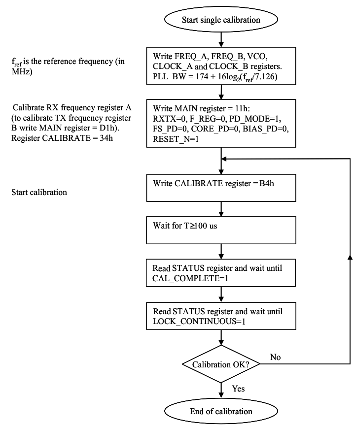
The single calibration algorithm (CAL_DUAL=0) using separate calibration for RX and TX frequency is illustrated in Figure 5-26. The same algorithm is applicable for dual calibration if CAL_DUAL=1.
TI recommends that single calibration be used for more robust operation.
There is a finite possibility that the PLL self-calibration will fail. The calibration routine in the source code should include a loop so that the PLL is re-calibrated until PLL lock is achieved if the PLL does not lock the first time. Refer to CC1021 Errata Note 002, available in the CC1021 product folder.
 Figure 5-26 Single Calibration Algorithm for RX and TX