SWRS108B May 2011 – June 2014 CC113L
PRODUCTION DATA.
- 1Device Overview
- 2Revision History
- 3Terminal Configuration and Functions
-
4Specifications
- 4.1 Absolute Maximum Ratings
- 4.2 Handling Ratings
- 4.3 Recommended Operating Conditions
- 4.4 General Characteristics
- 4.5 Current Consumption
- 4.6 RF Receive Section
- 4.7 Crystal Oscillator
- 4.8 Frequency Synthesizer Characteristics
- 4.9 DC Characteristics
- 4.10 Power-On Reset
- 4.11 Thermal Characteristics
- 4.12 Typical Characteristics
-
5Detailed Description
- 5.1 Overview
- 5.2 Functional Block Diagram
- 5.3 Configuration Overview
- 5.4 Configuration Software
- 5.5 4-wire Serial Configuration and Data Interface
- 5.6 Microcontroller Interface and Pin Configuration
- 5.7 Data Rate Programming
- 5.8 Receiver Channel Filter Bandwidth
- 5.9 Demodulator, Symbol Synchronizer, and Data Decision
- 5.10 Packet Handling Hardware Support
- 5.11 Modulation Formats
- 5.12 Received Signal Qualifiers and RSSI
- 5.13 Radio Control
- 5.14 RX FIFO
- 5.15 Frequency Programming
- 5.16 VCO
- 5.17 Voltage Regulators
- 5.18 General Purpose and Test Output Control Pins
- 5.19 Asynchronous and Synchronous Serial Operation
- 5.20 System Consideration and Guidelines
- 5.21 Configuration Registers
- 5.22 Development Kit Ordering Information
- 6Applications, Implementation, and Layout
- 7Device and Documentation Support
- 8Mechanical Packaging and Orderable Information
Package Options
Mechanical Data (Package|Pins)
- RGP|20
Thermal pad, mechanical data (Package|Pins)
- RGP|20
Orderable Information
4 Specifications
4.1 Absolute Maximum Ratings
Under no circumstances must the absolute maximum ratings be violated. Stress exceeding one or more of the limiting values may cause permanent damage to the device.| Parameter | Min | Max | Units | Condition |
|---|---|---|---|---|
| Supply voltage | –0.3 | 3.9 | V | All supply pins must have the same voltage |
| Voltage on any digital pin | –0.3 | VDD + 0.3, max 3.9 | V | |
| Voltage on the pins RF_P, RF_N, DCOUPL, RBIAS | –0.3 | 2.0 | V | |
| Voltage ramp-up rate | 120 | kV/µs | ||
| Input RF level | +10 | dBm |
4.2 Handling Ratings
| Parameter | MIN | MAX | UNIT | |
|---|---|---|---|---|
| Storage temperature range, Tstg | (default) | –50 | 150 | °C |
| ESD Stress Voltage, VESD | Human Body Model (HBM), per ANSI/ESDA/JEDEC JS001(1) | 750 | V | |
| Charged Device Model (CDM), per JJESD22-C101(2) | 400 | V |
(1) JEDEC document JEP155 states that 500-V HBM allows safe manufacturing with a standard ESD control process.
(2) JEDEC document JEP157 states that 250-V HBM allows safe manufacturing with a standard ESD control process.
4.3 Recommended Operating Conditions
| Parameter | Min | Max | Unit | Condition |
|---|---|---|---|---|
| Operating temperature | –40 | 85 | °C | |
| Operating supply voltage | 1.8 | 3.6 | V | All supply pins must have the same voltage |
4.4 General Characteristics
| Parameter | Min | Typ | Max | Unit | Condition |
|---|---|---|---|---|---|
| Frequency range | 300 | 348 | MHz | ||
| 387 | 464 | MHz | If using a 27 MHz crystal, the lower frequency limit for this band is 392 MHz | ||
| 779 | 928 | MHz | |||
| Data rate | 0.6 | 500 | kBaud | 2-FSK | |
| 0.6 | 250 | kBaud | GFSK and OOK | ||
| 0.6 | 300 | kBaud | 4-FSK (the data rate in kbps will be twice the baud rate) Optional Manchester encoding (the data rate in kbps will be half the baud rate) |
4.5 Current Consumption
TA = 25°C, VDD = 3.0 V if nothing else stated. All measurement results are obtained using SWRR046 and SWRR045. Reduced current settings, MDMCFG2.DEM_DCFILT_OFF=1, gives a slightly lower current consumption at the cost of a reduction in sensitivity. See Section 4.6 for additional details on current consumption and sensitivity.| Parameter | Min | Typ | Max | Unit | Condition |
|---|---|---|---|---|---|
| Current consumption in power down modes | 0.2 | 1 | µA | Voltage regulator to digital part off, register values retained (SLEEP state). All GDO pins programmed to 0x2F (HW to 0) | |
| 100 | µA | Voltage regulator to digital part off, register values retained, XOSC running (SLEEP state with MCSM0.OSC_FORCE_ON set) | |||
| 165 | µA | Voltage regulator to digital part on, all other modules in power down (XOFF state) | |||
| Current consumption | 1.7 | mA | Only voltage regulator to digital part and crystal oscillator running (IDLE state) | ||
| 8.4 | mA | The current consumption for the intermediate states when going from IDLE to RX, including the calibration state | |||
| Current consumption, 315 MHz |
15.4 | mA | Receive mode, 1.2 kBaud, reduced current, input at sensitivity limit | ||
| 14.4 | mA | Receive mode, 1.2 kBaud, register settings optimized for reduced current, input well above sensitivity limit | |||
| 15.2 | mA | Receive mode, 38.4 kBaud, register settings optimized for reduced current, input at sensitivity limit | |||
| 14.3 | mA | Receive mode, 38.4 kBaud, register settings optimized for reduced current, input well above sensitivity limit | |||
| 16.5 | mA | Receive mode, 250 kBaud, register settings optimized for reduced current, input at sensitivity limit | |||
| 15.1 | mA | Receive mode, 250 kBaud, register settings optimized for reduced current, input well above sensitivity limit | |||
| Current consumption, 433 MHz |
16.0 | mA | Receive mode, 1.2 kBaud, register settings optimized for reduced current, input at sensitivity limit | ||
| 15.0 | mA | Receive mode, 1.2 kBaud, register settings optimized for reduced current, input well above sensitivity limit | |||
| 15.7 | mA | Receive mode, 38.4 kBaud, register settings optimized for reduced current, input at sensitivity limit | |||
| 15.0 | mA | Receive mode, 38.4 kBaud, register settings optimized for reduced current, input well above sensitivity limit | |||
| 17.1 | mA | Receive mode, 250 kBaud, register settings optimized for reduced current, input at sensitivity limit | |||
| 15.7 | mA | Receive mode, 250 kBaud, register settings optimized for reduced current, input well above sensitivity limit | |||
| Current consumption, 868/915 MHz |
15.7 | mA | Receive mode, 1.2 kBaud, register settings optimized for reduced current, input at sensitivity limit. See Figure 4-1 through Figure 4-3 for current consumption with register settings optimized for sensitivity. |
||
| 14.7 | mA | Receive mode, 1.2 kBaud, register settings optimized for reduced current, input well above sensitivity limit. See Figure 4-1 through Figure 4-3 for current consumption with register settings optimized for sensitivity. |
|||
| 15.6 | mA | Receive mode, 38.4 kBaud, register settings optimized for reduced current, input at sensitivity limit. See Figure 4-1 through Figure 4-3 for current consumption with register settings optimized for sensitivity. |
|||
| 14.6 | mA | Receive mode, 38.4 kBaud, register settings optimized for reduced current, input well above sensitivity limit. See Figure 4-1 through Figure 4-3 for current consumption with register settings optimized for sensitivity. |
|||
| 16.9 | mA | Receive mode, 250 kBaud, register settings optimized for reduced current, input at sensitivity limit. See Figure 4-1 through Figure 4-3 for current consumption with register settings optimized for sensitivity. |
|||
| 15.6 | mA | Receive mode, 250 kBaud, register settings optimized for reduced current, input well above sensitivity limit. See Figure 4-1 through Figure 4-3 for current consumption with register settings optimized for sensitivity. |
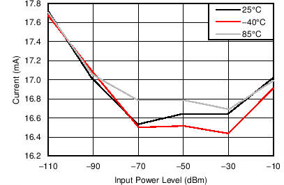
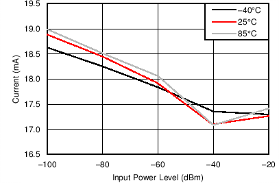
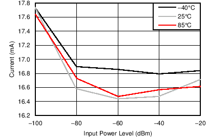
4.5.1 Typical RX Current Consumption over Temperature and Input Power Level, 868/915 MHz
See Section 4.12.1.
4.6 RF Receive Section
TA = 25°C, VDD = 3.0 V if nothing else stated. All measurement results are obtained using SWRR046 and SWRR045.
| Parameter | Min | Typ | Max | Unit | Condition |
|---|---|---|---|---|---|
| Digital channel filter bandwidth | 58 | 812 | kHz | User programmable. The bandwidth limits are proportional to crystal frequency (given values assume a 26.0 MHz crystal) | |
| Spurious emissions | –68 | –57 | dBm | 25 MHz - 1 GHz | |
| (Maximum figure is the ETSI EN 300 220 V2.3.1 limit) | |||||
| –66 | –47 | dBm | Above 1 GHz | ||
| (Maximum figure is the ETSI EN 300 220 V2.3.1 limit) | |||||
| Typical radiated spurious emission is –49 dBm measured at the VCO frequency | |||||
| RX latency | 9 | bit | Serial operation. Time from start of reception until data is available on the receiver data output pin is equal to 9 bit | ||
| 315 MHz | |||||
| 1.2 kBaud data rate, sensitivity optimized, MDMCFG2.DEM_DCFILT_OFF=0 | |||||
| (2-FSK, 1% packet error rate, 20 bytes packet length, 5.2 kHz deviation, 58 kHz digital channel filter bandwidth) | |||||
| Receiver sensitivity | –111 | dBm | Sensitivity can be traded for current consumption by setting MDMCFG2.DEM_DCFILT_OFF=1. The typical current consumption is then reduced from 17.2 mA to 15.4 mA at the sensitivity limit. The sensitivity is typically reduced to -109 dBm | ||
| 433 MHz | |||||
| 0.6 kBaud data rate, sensitivity optimized, MDMCFG2.DEM_DCFILT_OFF=0 | |||||
| (GFSK, 1% packet error rate, 20 bytes packet length, 14.3 kHz deviation, 58 kHz digital channel filter bandwidth) | |||||
| Receiver sensitivity | –116 | dBm | |||
| 1.2 kBaud data rate, sensitivity optimized, MDMCFG2.DEM_DCFILT_OFF=0 | |||||
| GFSK, 1% packet error rate, 20 bytes packet length, 5.2 kHz deviation, 58 kHz digital channel filter bandwidth) | |||||
| Receiver sensitivity | –112 | dBm | Sensitivity can be traded for current consumption by setting MDMCFG2.DEM_DCFILT_OFF=1. The typical current consumption is then reduced from 18.0 mA to 16.0 mA at the sensitivity limit. The sensitivity is typically reduced to –110 dBm | ||
| 38.4 kBaud data rate, sensitivity optimized, MDMCFG2.DEM_DCFILT_OFF=0 | |||||
| (GFSK, 1% packet error rate, 20 bytes packet length, 20 kHz deviation, 100 kHz digital channel filter bandwidth) | |||||
| Receiver sensitivity | –104 | dBm | |||
| 250 kBaud data rate, sensitivity optimized, MDMCFG2.DEM_DCFILT_OFF=0 | |||||
| (GFSK, 1% packet error rate, 20 bytes packet length, 127 kHz deviation, 540 kHz digital channel filter bandwidth) | |||||
| Receiver sensitivity | –95 | dBm | |||
| 868/915 MHz | |||||
| 1.2 kBaud data rate, sensitivity optimized, MDMCFG2.DEM_DCFILT_OFF=0 | |||||
| (GFSK, 1% packet error rate, 20 bytes packet length, 5.2 kHz deviation, 58 kHz digital channel filter bandwidth) | |||||
| Receiver sensitivity | –112 | dBm | Sensitivity can be traded for current consumption by setting MDMCFG2.DEM_DCFILT_OFF=1. The typical current consumption is then reduced from 17.7 mA to 15.7 mA at sensitivity limit. The sensitivity is typically reduced to –109 dBm | ||
| Saturation | –14 | dBm | FIFOTHR.CLOSE_IN_RX=0. See more in DN010 SWRA147 | ||
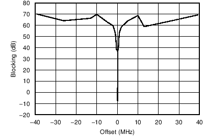
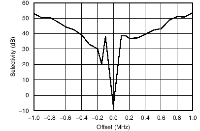
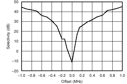
| Adjacent channel rejection ±100 kHz offset | 37 | dB | Desired channel 3 dB above the sensitivity limit. 100 kHz channel spacing See Figure 4-4 and Figure 4-5 for selectivity performance at other offset frequencies |
||
| Image channel rejection | 31 | dB | IF frequency 152 kHz Desired channel 3 dB above the sensitivity limit |
||
| Blocking | Desired channel 3 dB above the sensitivity limit See Figure 4-4 and Figure 4-5 for blocking performance at other offset frequencies |
||||
| ±2 MHz offset | –50 | dBm | |||
| ±10 MHz offset | –40 | dBm | |||
| 38.4 kBaud data rate, sensitivity optimized, MDMCFG2.DEM_DCFILT_OFF=0 | |||||
| (GFSK, 1% packet error rate, 20 bytes packet length, 20 kHz deviation, 100 kHz digital channel filter bandwidth) | |||||
| Receiver sensitivity | –104 | dBm | Sensitivity can be traded for current consumption by setting MDMCFG2.DEM_DCFILT_OFF=1. The typical current consumption is then reduced from 17.7 mA to 15.6 mA at the sensitivity limit. The sensitivity is typically reduced to -102 dBm | ||
| Saturation | –16 | dBm | FIFOTHR.CLOSE_IN_RX=0. See more in DN010 SWRA147 | ||
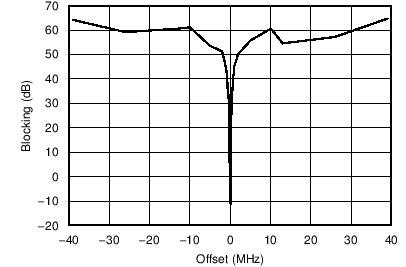
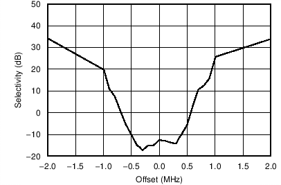
| Adjacent channel rejection | Desired channel 3 dB above the sensitivity limit. 200 kHz channel spacing See Figure 4-6 and Figure 4-7 for blocking performance at other offset frequencies |
||||
| –200 kHz offset | 12 | dB | |||
| +200 kHz offset | 25 | dB | |||
| Image channel rejection | 23 | dB | IF frequency 152 kHz Desired channel 3 dB above the sensitivity limit |
||
| Blocking | Desired channel 3 dB above the sensitivity limit See Figure 4-6 and Figure 4-7 for blocking performance at other offset frequencies |
||||
| ±2 MHz offset | –50 | dBm | |||
| ±10 MHz offset | –40 | dBm | |||
| 250 kBaud data rate, sensitivity optimized, MDMCFG2.DEM_DCFILT_OFF=0 | |||||
| (GFSK, 1% packet error rate, 20 bytes packet length, 127 kHz deviation, 540 kHz digital channel filter bandwidth) | |||||
| Receiver sensitivity | –95 | dBm | Sensitivity can be traded for current consumption by setting MDMCFG2.DEM_DCFILT_OFF=1. The typical current consumption is then reduced from 18.9 mA to 16.9 mA at the sensitivity limit. The sensitivity is typically reduced to -91 dBm | ||
| Saturation | –17 | dBm | FIFOTHR.CLOSE_IN_RX=0. See more in DN010 SWRA147 | ||
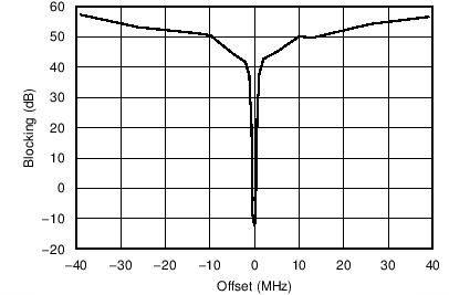
| Adjacent channel rejection | 25 | dB | Desired channel 3 dB above the sensitivity limit. 750-kHz channel spacing See Figure 4-8 and Figure 4-9 for blocking performance at other offset frequencies |
||
| Image channel rejection | 14 | dB | IF frequency 304 kHz Desired channel 3 dB above the sensitivity limit |
||
| Blocking | Desired channel 3 dB above the sensitivity limit See Figure 4-8 and Figure 4-9 for blocking performance at other offset frequencies |
||||
| ±2 MHz offset | –50 | dBm | |||
| ±10 MHz offset | –40 | dBm | |||
| 4-FSK, 125 kBaud data rate (250 kbps), sensitivity optimized, MDMCFG2.DEM_DCFILT_OFF=0 | |||||
| (1% packet error rate, 20 bytes packet length, 127 kHz deviation, 406 kHz digital channel filter bandwidth) | |||||
| Receiver sensitivity | –96 | dBm | |||
| 4-FSK, 250 kBaud data rate (500 kbps), sensitivity optimized, MDMCFG2.DEM_DCFILT_OFF=0 | |||||
| (1% packet error rate, 20 bytes packet length, 254 kHz deviation, 812 kHz digital channel filter bandwidth | |||||
| Receiver sensitivity | –91 | dBm | |||
| 4-FSK, 300 kBaud data rate (600 kbps), sensitivity optimized, MDMCFG2.DEM_DCFILT_OFF=0 | |||||
| (1% packet error rate, 20 bytes packet length, 228 kHz deviation, 812 kHz digital channel filter bandwidth) | |||||
| Receiver sensitivity | –89 | dBm | |||
4.6.1 Typical Sensitivity over Temperature and Supply Voltage, 868 MHz, Sensitivity Optimized Setting
| Supply Voltage | Supply Voltage | Supply Voltage | |||||||
|---|---|---|---|---|---|---|---|---|---|
| VDD = 1.8 V | VDD = 3.0 V | VDD = 3.6 V | |||||||
| Temperature [°C] | –40 | 25 | 85 | –40 | 25 | 85 | –40 | 25 | 85 |
| Sensitivity [dBm] 1.2 kBaud | –113 | –112 | –110 | –113 | –112 | –110 | –113 | –112 | –110 |
| Sensitivity [dBm] 38.4 kBaud | –105 | –104 | –102 | –105 | –104 | –102 | –105 | –104 | –102 |
| Sensitivity [dBm] 250 kBaud | –97 | –96 | –92 | –97 | –95 | –92 | –97 | –94 | –92 |
| Sensitivity [dBm] 500 kBaud | –91 | –90 | –86 | –91 | –90 | –86 | –91 | –90 | –86 |
4.6.2 Typical Sensitivity over Temperature and Supply Voltage, 915 MHz, Sensitivity Optimized Setting
| Supply Voltage | Supply Voltage | Supply Voltage | |||||||
|---|---|---|---|---|---|---|---|---|---|
| VDD = 1.8 V | VDD = 3.0 V | VDD = 3.6 V | |||||||
| Temperature [°C] | –40 | 25 | 85 | –40 | 25 | 85 | –40 | 25 | 85 |
| Sensitivity [dBm] 1.2 kBaud | –113 | –112 | –110 | –113 | –112 | –110 | –113 | –112 | –110 |
| Sensitivity [dBm] 38.4 kBaud | –105 | –104 | –102 | –104 | –104 | –102 | –105 | –104 | –102 |
| Sensitivity [dBm] 250 kBaud | –97 | –94 | –92 | –97 | –95 | –92 | –97 | –95 | –92 |
| Sensitivity [dBm] 500 kBaud | –91 | –89 | –86 | –91 | –90 | –86 | –91 | –89 | –86 |
4.6.3 Blocking and Selectivity
See Section 4.12.2.
4.7 Crystal Oscillator
TA = 25°C, VDD = 3.0 V if nothing else is stated. All measurement results obtained using SWRR046 and SWRR045.| Parameter | Min | Typ | Max | Unit | Condition |
|---|---|---|---|---|---|
| Crystal frequency | 26 | 26 | 27 | MHz | For compliance with modulation bandwidth requirements under EN 300 220 V2.3.1 in the 863 to 870 MHz frequency range it is recommended to use a 26-MHz crystal for frequencies below 869 MHz and a 27 MHz crystal for frequencies above 869 MHz. |
| Tolerance | ±40 | ppm | This is the total tolerance including a) initial tolerance, b) crystal loading, c) aging, and d) temperature dependence. The acceptable crystal tolerance depends on RF frequency and channel spacing / bandwidth. | ||
| Load capacitance | 10 | 13 | 20 | pF | Simulated over operating conditions |
| ESR | 100 | Ω | |||
| Start-up time | 150 | µs | This parameter is to a large degree crystal dependent. Measured on SWRR046 and SWRR045 using crystal AT-41CD2 from NDK |
4.8 Frequency Synthesizer Characteristics
TA = 25°C, VDD = 3.0 V if nothing else is stated. All measurement results are obtained using SWRR046 and SWRR045. Min figures are given using a 27-MHz crystal. Typ and max figures are given using a 26-MHz crystal.| Parameter | Min | Typ | Max | Unit | Condition |
|---|---|---|---|---|---|
| Programmed frequency resolution | 397 | FXOSC/216 | 412 | Hz | 26- to 27-MHz crystal. The resolution (in Hz) is equal for all frequency bands |
| Synthesizer frequency tolerance | ±40 | ppm | Given by crystal used. Required accuracy (including temperature and aging) depends on frequency band and channel bandwidth / spacing | ||
| RF carrier phase noise | –92 | dBc/Hz | at 50 kHz offset from carrier | ||
| RF carrier phase noise | –92 | dBc/Hz | at 100 kHz offset from carrier | ||
| RF carrier phase noise | –92 | dBc/Hz | at 200 kHz offset from carrier | ||
| RF carrier phase noise | –98 | dBc/Hz | at 500 kHz offset from carrier | ||
| RF carrier phase noise | –107 | dBc/Hz | at 1 MHz offset from carrier | ||
| RF carrier phase noise | –113 | dBc/Hz | at 2 MHz offset from carrier | ||
| RF carrier phase noise | –119 | dBc/Hz | at 5 MHz offset from carrier | ||
| RF carrier phase noise | –129 | dBc/Hz | at 10 MHz offset from carrier | ||
| PLL turn-on or hop time (See Table 5-12) |
72 | 75 | 75 | µs | Time from leaving the IDLE state until arriving in the RX state, when not performing calibration. Crystal oscillator running. |
| PLL calibration time (See Table 5-13) |
685 | 712 | 724 | µs | Calibration can be initiated manually or automatically before entering or after leaving RX |
4.9 DC Characteristics
TA = 25°C if nothing else stated.| Digital Inputs/Outputs | Min | Max | Unit | Condition |
|---|---|---|---|---|
| Logic "0" input voltage | 0 | 0.7 | V | |
| Logic "1" input voltage | VDD – 0.7 | VDD | V | |
| Logic "0" output voltage | 0 | 0.5 | V | For up to 4 mA output current |
| Logic "1" output voltage | VDD – 0.3 | VDD | V | For up to 4 mA output current |
| Logic "0" input current | N/A | –50 | nA | Input equals 0 V |
| Logic "1" input current | N/A | 50 | nA | Input equals VDD |
4.10 Power-On Reset
For proper Power-On-Reset functionality the power supply should comply with the requirements in Section 4.10. Otherwise, the chip should be assumed to have unknown state until transmitting an SRES strobe over the SPI interface. See Section 5.13.1, Power-On Start-Up Sequence, for further details.| Parameter | Min | Typ | Max | Unit | Condition |
|---|---|---|---|---|---|
| Power-up ramp-up time | 5 | ms | From 0 V until reaching 1.8 V | ||
| Power off time | 1 | ms | Minimum time between power-on and power-off |
4.11 Thermal Characteristics(1)
| NAME | DESCRIPTION | QFN (°C/W) |
|---|---|---|
| RθJA | Junction-to-ambient thermal resistance | 47 |
| RθJC(top) | Junction-to-case (top) thermal resistance | 45 |
| RθJB | Junction-to-board thermal resistance | 13.6 |
| RθJC(bot) | Junction-to-case (bottom) thermal resistance | 5.12 |
(1) For more information about traditional and new thermal metrics, see the IC Package Thermal Metrics application report, SPRA953.
4.12 Typical Characteristics
4.12.1 Typical Characteristics, RX Current Consumption
4.12.2 Typical Characteristics, Blocking and Selectivity