SWRS108B May 2011 – June 2014 CC113L
PRODUCTION DATA.
- 1Device Overview
- 2Revision History
- 3Terminal Configuration and Functions
-
4Specifications
- 4.1 Absolute Maximum Ratings
- 4.2 Handling Ratings
- 4.3 Recommended Operating Conditions
- 4.4 General Characteristics
- 4.5 Current Consumption
- 4.6 RF Receive Section
- 4.7 Crystal Oscillator
- 4.8 Frequency Synthesizer Characteristics
- 4.9 DC Characteristics
- 4.10 Power-On Reset
- 4.11 Thermal Characteristics
- 4.12 Typical Characteristics
-
5Detailed Description
- 5.1 Overview
- 5.2 Functional Block Diagram
- 5.3 Configuration Overview
- 5.4 Configuration Software
- 5.5 4-wire Serial Configuration and Data Interface
- 5.6 Microcontroller Interface and Pin Configuration
- 5.7 Data Rate Programming
- 5.8 Receiver Channel Filter Bandwidth
- 5.9 Demodulator, Symbol Synchronizer, and Data Decision
- 5.10 Packet Handling Hardware Support
- 5.11 Modulation Formats
- 5.12 Received Signal Qualifiers and RSSI
- 5.13 Radio Control
- 5.14 RX FIFO
- 5.15 Frequency Programming
- 5.16 VCO
- 5.17 Voltage Regulators
- 5.18 General Purpose and Test Output Control Pins
- 5.19 Asynchronous and Synchronous Serial Operation
- 5.20 System Consideration and Guidelines
- 5.21 Configuration Registers
- 5.22 Development Kit Ordering Information
- 6Applications, Implementation, and Layout
- 7Device and Documentation Support
- 8Mechanical Packaging and Orderable Information
Package Options
Mechanical Data (Package|Pins)
- RGP|20
Thermal pad, mechanical data (Package|Pins)
- RGP|20
Orderable Information
6 Applications, Implementation, and Layout
Figure 5-1 shows the low cost CC113LEM application circuit (see SWRR083 and SWRR084) (see Table 6-1 for component values).
The designs in SWRR046 and SWRR045 were used for CC113L characterization. The application circuits are shown in Figure 6-2 and Figure 6-3 (see Table 6-1 for component values).
6.1 Bias Resistor
The 56-kΩ bias resistor R171 is used to set an accurate bias current.
6.2 Balun and RF Matching
The balun component values and their placement are important to keep the performance optimized. Gerber files and schematics for the reference designs are available for download from the TI website.
6.2.1 Balun and RF Matching (Low-Cost Application Circuit)
The components between the RF_N/RF_P pins and the point where the two signals are joined together (C131, C122, L122, and L132, see Figure 6-1) form a balun that converts singleended RF signal at the antenna to a differential RF signal on CC113L. C124 is needed for DC blocking.
The balun components also matches the CC113L input impedance to a 50-Ω source. C126 provides DC blocking and is only needed if there is a DC path in the antenna.
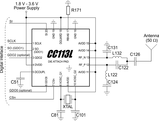 Figure 6-1 Low Cost Application Circuit and Evaluation Circuit 315, 433, 868, or 915 MHz (Excluding Supply Decoupling Capacitors)
Table 6-1 External Components (Low-Cost Application Circuit
| Component | Value at 315 MHz | Value at 433 MHz | Value at 868/915 MHz |
|---|---|---|---|
| C124 | 220 pF | 220 pF | 100 pF |
| C122 | 6.8 pF | 3.9 pF | 2.2 pF |
| C126 | 220 pF | 220 pF | 100 pF |
| C131 | 6.8 pF | 3.9 pF | 2.2 pF |
| L122 | 33 nH | 27 nH | 12 nH |
| L132 | 33 nH | 27 nH | 12 nH |
6.2.2 Balun and RF Matching (Characterization Circuit)
The components between the RF_N/RF_P pins and the point where the two signals are joined together (C131, C122, L122, and L132 in Figure 6-2 and L121, L131, C121, L122, C131, C122, and L132 in Figure 6-3) form a balun that converts single-ended RF signal at the antenna to a differential RF signal on CC113L. C124 is needed for DC blocking.
The balun components also matches the CC113L input impedance to a 50-Ω source. C126 provides DC blocking and is only needed if there is a DC path in the antenna.
Note that the 315/433 MHz design SWRR046 uses Murata LQG15 multi-layer inductors while the 868/915 MHz design SWRR045 uses Murata LQW15 wire-wound inductors.
L123, L124, and C123 (plus C125 in Figure 6-2) form an LC low-pass filter. This filter is not required for an RX-only design and can be omitted.
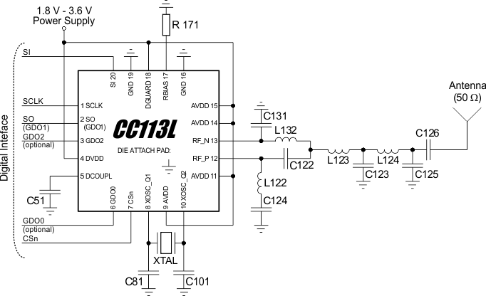 Figure 6-2 Characterization Circuit 315 and 433 MHz (Excluding Supply Decoupling Capacitors)
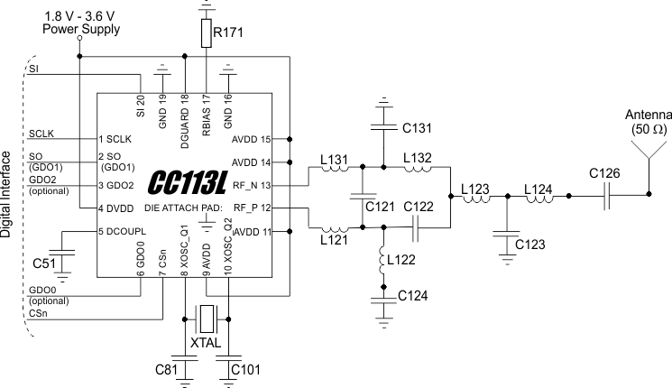 Figure 6-3 Characterization Circuit 868 and 915 MHz (Excluding Supply Decoupling Capacitors)
Table 6-2 External Components
| Component | Value at 315 MHz | Value at 433 MHz | Value at 868/915 MHz |
|---|---|---|---|
| C121 | 1 pF | ||
| C122 | 6.8 pF | 3.9 pF | 1.5 pF |
| C123 | 12 pF | 8.2 pF | 3.3 pF |
| C124 | 220 pF | 220 pF | 100 pF |
| C125 | 6.8 pF | 5.6 pF | |
| C126 | 220 pF | 220 pF | 100 pF |
| C131 | 6.8 pF | 3.9 pF | 1.5 pF |
| L121 | 12 nH | ||
| L122 | 33 nH | 27 nH | 18 nH |
| L123 | 18 nH | 22 nH | 12 nH |
| L124 | 33 nH | 27 nH | 12 nH |
| L131 | 12 nH | ||
| L132 | 33 nH | 27 nH | 18 nH |
6.3 Crystal
A crystal in the frequency range 26 - 27 MHz must be connected between the XOSC_Q1 and XOSC_Q2 pins. The oscillator is designed for parallel mode operation of the crystal. In addition, loading capacitors (C81 and C101) for the crystal are required. The loading capacitor values depend on the total load capacitance, CL, specified for the crystal. The total load capacitance seen between the crystal terminals should equal CL for the crystal to oscillate at the specified frequency.
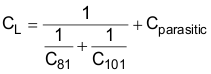
The parasitic capacitance is constituted by pin input capacitance and PCB stray capacitance. Total parasitic capacitance is typically 2.5 pF.
The crystal oscillator is amplitude regulated. This means that a high current is used to start up the oscillations. When the amplitude builds up, the current is reduced to what is necessary to maintain approximately 0.4 Vpp signal swing. This ensures a fast start-up, and keeps the drive level to a minimum. The ESR of the crystal should be within the specification in order to ensure a reliable start-up (see Section 4.7).
The initial tolerance, temperature drift, aging and load pulling should be carefully specified in order to meet the required frequency accuracy in a certain application.
Avoid routing digital signals with sharp edges close to XOSC_Q1 PCB track or underneath the crystal Q1 pad as this may shift the crystal dc operating point and result in duty cycle variation.
6.4 Reference Signal
The chip can alternatively be operated with a reference signal from 26 to 27 MHz instead of a crystal. This input clock can either be a full-swing digital signal (0 V to VDD) or a sine wave of maximum 1 V peak-peak amplitude. The reference signal must be connected to the XOSC_Q1 input. The sine wave must be connected to XOSC_Q1 using a serial capacitor. When using a full-swing digital signal, this capacitor can be omitted. The XOSC_Q2 line must be left un-connected. C81 and C101 can be omitted when using a reference signal.
6.5 Power Supply Decoupling
The power supply must be properly decoupled close to the supply pins. Note that decoupling capacitors are not shown in the application circuit. The placement and the size of the decoupling capacitors are very important to achieve the optimum performance. The CC113LEM reference designs SWRR081 and SWRR082 should be followed closely.
6.6 PCB Layout Recommendations
The top layer should be used for signal routing, and the open areas should be filled with metallization connected to ground using several vias.
The area under the chip is used for grounding and shall be connected to the bottom ground plane with several vias for good thermal performance and sufficiently low inductance to ground.
In the CC113LEM reference designs, SWRR081 and SWRR082, 5 vias are placed inside the exposed die attached pad. These vias should be “tented” (covered with solder mask) on the component side of the PCB to avoid migration of solder through the vias during the solder reflow process.
The solder paste coverage should not be 100%. If it is, out gassing may occur during the reflow process, which may cause defects (splattering, solder balling). Using “tented” vias reduces the solder paste coverage below 100%. See Figure 6-4 for top solder resist and top paste masks.
Each decoupling capacitor should be placed as close as possible to the supply pin it is supposed to decouple. Each decoupling capacitor should be connected to the power line (or power plane) by separate vias. The best routing is from the power line (or power plane) to the decoupling capacitor and then to the CC113L supply pin. Supply power filtering is very important.
Each decoupling capacitor ground pad should be connected to the ground plane by separate vias. Direct connections between neighboring power pins will increase noise coupling and should be avoided unless absolutely necessary. Routing in the ground plane underneath the chip or the balun/RF matching circuit, or between the chip’s ground vias and the decoupling capacitor’s ground vias should be avoided. This improves the grounding and ensures the shortest possible current return path.
Avoid routing digital signals with sharp edges close to XOSC_Q1 PCB track or underneath the crystal Q1 pad as this may shift the crystal dc operating point and result in duty cycle variation.
The external components should ideally be as small as possible (0402 is recommended) and surface mount devices are highly recommended. Components with different sizes than those specified may have differing characteristics.
Precaution should be used when placing the microcontroller in order to avoid noise interfering with the RF circuitry.
A CC11xL Development Kit with a fully assembled CC113L Evaluation Module is available. It is strongly advised that this reference layout is followed very closely in order to get the best performance. The schematic, BOM and layout Gerber files are all available from the TI website (SWRR081 and SWRR082).
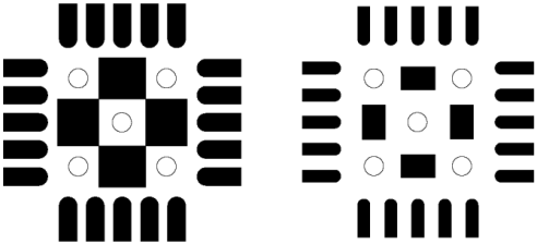 Figure 6-4 Left: Top Solder Resist Mask (Negative) – Right: Top Paste Mask. Circles are Vias