SWRS108B May 2011 – June 2014 CC113L
PRODUCTION DATA.
- 1Device Overview
- 2Revision History
- 3Terminal Configuration and Functions
-
4Specifications
- 4.1 Absolute Maximum Ratings
- 4.2 Handling Ratings
- 4.3 Recommended Operating Conditions
- 4.4 General Characteristics
- 4.5 Current Consumption
- 4.6 RF Receive Section
- 4.7 Crystal Oscillator
- 4.8 Frequency Synthesizer Characteristics
- 4.9 DC Characteristics
- 4.10 Power-On Reset
- 4.11 Thermal Characteristics
- 4.12 Typical Characteristics
-
5Detailed Description
- 5.1 Overview
- 5.2 Functional Block Diagram
- 5.3 Configuration Overview
- 5.4 Configuration Software
- 5.5 4-wire Serial Configuration and Data Interface
- 5.6 Microcontroller Interface and Pin Configuration
- 5.7 Data Rate Programming
- 5.8 Receiver Channel Filter Bandwidth
- 5.9 Demodulator, Symbol Synchronizer, and Data Decision
- 5.10 Packet Handling Hardware Support
- 5.11 Modulation Formats
- 5.12 Received Signal Qualifiers and RSSI
- 5.13 Radio Control
- 5.14 RX FIFO
- 5.15 Frequency Programming
- 5.16 VCO
- 5.17 Voltage Regulators
- 5.18 General Purpose and Test Output Control Pins
- 5.19 Asynchronous and Synchronous Serial Operation
- 5.20 System Consideration and Guidelines
- 5.21 Configuration Registers
- 5.22 Development Kit Ordering Information
- 6Applications, Implementation, and Layout
- 7Device and Documentation Support
- 8Mechanical Packaging and Orderable Information
Package Options
Mechanical Data (Package|Pins)
- RGP|20
Thermal pad, mechanical data (Package|Pins)
- RGP|20
Orderable Information
3 Terminal Configuration and Functions
3.1 Pin Diagram
The CC113L pinout is shown in Figure 3-1 and Table 3-1. See Section 5.18 for details on the I/O configuration.
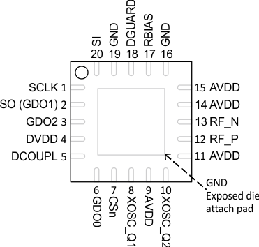 Figure 3-1 Pinout Top View
NOTE
The exposed die attach pad must be connected to a solid ground plane as this is the main ground connection for the chip
3.2 Signal Descriptions
Table 3-1 Signal Descriptions
| Pin No. | Pin Name | Pin Type | Description |
|---|---|---|---|
| 1 | SCLK | Digital Input | Serial configuration interface, clock input |
| 2 | SO (GDO1) | Digital Output | Serial configuration interface, data output |
| Optional general output pin when CSn is high | |||
| 3 | GDO2 | Digital Output | Digital output pin for general use:
|
| 4 | DVDD | Power (Digital) | 1.8 - 3.6 V digital power supply for digital I/Os and for the digital core voltage regulator |
| 5 | DCOUPL | Power (Digital) | 1.6 - 2.0 V digital power supply output for decoupling |
|
NOTE: This pin is intended for use with the CC113L only. It can not be used to provide supply voltage to other devices |
|||
| 6 | GDO0 | Digital I/O | Digital output pin for general use:
|
| 7 | CSn | Digital Input | Serial configuration interface, chip select |
| 8 | XOSC_Q1 | Analog I/O | Crystal oscillator pin 1, or external clock input |
| 9 | AVDD | Power (Analog) | 1.8 - 3.6 V analog power supply connection |
| 10 | XOSC_Q2 | Analog I/O | Crystal oscillator pin 2 |
| 11 | AVDD | Power (Analog) | 1.8 - 3.6 V analog power supply connection |
| 12 | RF_P | RF I/O | Positive RF input signal to LNA in receive mode |
| 13 | RF_N | RF I/O | Negative RF input signal to LNA in receive mode |
| 14 | AVDD | Power (Analog) | 1.8 - 3.6 V analog power supply connection |
| 15 | AVDD | Power (Analog) | 1.8 - 3.6 V analog power supply connection |
| 16 | GND | Ground (Analog) | Analog ground connection |
| 17 | RBIAS | Analog I/O | External bias resistor for reference current |
| 18 | DGUARD | Power (Digital) | Power supply connection for digital noise isolation |
| 19 | GND | Ground (Digital) | Ground connection for digital noise isolation |
| 20 | SI | Digital Input | Serial configuration interface, data input |