SWAS037B February   2019  – May 2021 CC3135

PRODUCTION DATA  

  1. Features
  2. Applications
  3. Description
  4. Functional Block Diagram
  5. Revision History
  6. Device Comparison
    1. 6.1 Related Products
  7. Terminal Configuration and Functions
    1. 7.1 Pin Diagram
    2. 7.2 Pin Attributes
    3. 7.3 Signal Descriptions
      1.      12
    4. 7.4 Connections for Unused Pins
  8. Specifications
    1. 8.1  Absolute Maximum Ratings
    2. 8.2  ESD Ratings
    3. 8.3  Power-On Hours (POH)
    4. 8.4  Recommended Operating Conditions
    5. 8.5  Current Consumption Summary: 2.4 GHz RF Band
    6. 8.6  Current Consumption Summary: 5 GHz RF Band
    7. 8.7  TX Power Control for 2.4 GHz Band
    8. 8.8  TX Power Control for 5 GHz
    9. 8.9  Brownout and Blackout Conditions
      1.      24
    10. 8.10 Electrical Characteristics for DIO Pins
      1.      26
      2.      27
    11. 8.11 Electrical Characteristics for Pin Internal Pullup and Pulldown
    12. 8.12 WLAN Receiver Characteristics
      1.      30
      2.      31
    13. 8.13 WLAN Transmitter Characteristics
      1.      33
      2.      34
    14. 8.14 WLAN Transmitter Out-of-Band Emissions
      1.      36
      2.      37
    15. 8.15 BLE/2.4 GHz Radio Coexistence and WLAN Coexistence Requirements
    16. 8.16 Thermal Resistance Characteristics for RGK Package
    17. 8.17 Timing and Switching Characteristics
      1. 8.17.1 Power Supply Sequencing
      2. 8.17.2 Device Reset
      3. 8.17.3 Reset Timing
        1. 8.17.3.1 nRESET (32-kHz Crystal)
        2.       45
        3. 8.17.3.2 nRESET (External 32-kHz Crystal)
          1.        47
      4. 8.17.4 Wakeup From HIBERNATE Mode
        1.       49
      5. 8.17.5 Clock Specifications
        1. 8.17.5.1 Slow Clock Using Internal Oscillator
          1.        52
        2. 8.17.5.2 Slow Clock Using an External Clock
          1.        54
        3. 8.17.5.3 Fast Clock (Fref) Using an External Crystal
          1.        56
        4. 8.17.5.4 Fast Clock (Fref) Using an External Oscillator
          1.        58
      6. 8.17.6 Interfaces
        1. 8.17.6.1 Host SPI Interface Timing
          1.        61
        2. 8.17.6.2 Flash SPI Interface Timing
          1.        63
        3. 8.17.6.3 DIO Interface Timing
          1. 8.17.6.3.1 DIO Output Transition Time Parameters (Vsupply = 3.3 V)
            1.         66
          2. 8.17.6.3.2 DIO Input Transition Time Parameters
            1.         68
    18. 8.18 External Interfaces
      1. 8.18.1 SPI Flash Interface
      2. 8.18.2 SPI Host Interface
      3. 8.18.3 Host UART Interface
        1. 8.18.3.1 5-Wire UART Topology
        2. 8.18.3.2 4-Wire UART Topology
        3. 8.18.3.3 3-Wire UART Topology
  9. Detailed Description
    1. 9.1 Overview
    2. 9.2 Device Features
      1. 9.2.1 WLAN
      2. 9.2.2 Network Stack
      3. 9.2.3 Security
      4. 9.2.4 Host Interface and Driver
      5. 9.2.5 System
    3. 9.3 FIPS 140-2 Level 1 Certification
    4. 9.4 Power-Management Subsystem
      1. 9.4.1 VBAT Wide-Voltage Connection
    5. 9.5 Low-Power Operating Modes
      1. 9.5.1 Low-Power Deep Sleep
      2. 9.5.2 Hibernate
      3. 9.5.3 Shutdown
    6. 9.6 Memory
      1. 9.6.1 External Memory Requirements
    7. 9.7 Restoring Factory Default Configuration
    8. 9.8 Hostless Mode
  10. 10Applications, Implementation, and Layout
    1. 10.1 Application Information
      1. 10.1.1 BLE/2.4 GHz Radio Coexistence
      2. 10.1.2 Antenna Selection
      3. 10.1.3 Typical Application
    2. 10.2 PCB Layout Guidelines
      1. 10.2.1 General PCB Guidelines
      2. 10.2.2 Power Layout and Routing
        1. 10.2.2.1 Design Considerations
      3. 10.2.3 Clock Interface Guidelines
      4. 10.2.4 Digital Input and Output Guidelines
      5. 10.2.5 RF Interface Guidelines
  11. 11Device and Documentation Support
    1. 11.1  Third-Party Products Disclaimer
    2. 11.2  Tools and Software
    3. 11.3  Firmware Updates
    4. 11.4  Device Nomenclature
    5. 11.5  Documentation Support
    6. 11.6  Support Resources
    7. 11.7  Trademarks
    8. 11.8  Electrostatic Discharge Caution
    9. 11.9  Export Control Notice
    10. 11.10 Glossary
  12. 12Mechanical, Packaging, and Orderable Information
    1. 12.1 Packaging Information
    2. 12.2 Package Option Addendum
      1. 12.2.1 Packaging Information
      2. 12.2.2 Tape and Reel Information

Package Options

Mechanical Data (Package|Pins)
Thermal pad, mechanical data (Package|Pins)
Orderable Information

Fast Clock (Fref) Using an External Crystal

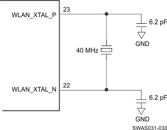
The CC3135 device also incorporates an internal crystal oscillator to support a crystal-based fast clock. The crystal is fed directly between WLAN_XTAL_P (pin 23) and WLAN_XTAL_N (pin 22) with suitable loading capacitors.

Figure 8-11 shows the crystal connections for the fast clock.
GUID-3988083E-2607-4A9A-915C-8B69D5633B60-low.gif
NOTE: The crystal capacitance must be tuned to ensure that the PPM requirement is met. See CC31xx & CC32xx Frequency Tuning for information on frequency tuning.
Figure 8-11 Fast Clock Crystal Connections


Table 8-16 lists the WLAN fast-clock crystal requirements.