SCLS569C January 2004 – April 2024 CD74HCT4051-Q1
PRODUCTION DATA
- 1
- 1Features
- 2Applications
- 3Description
- 4Pin Configuration and Functions
- 5Specifications
- 6Parameter Measurement Information
- 7Device and Documentation Support
- 8Revision History
- 9Mechanical, Packaging, and Orderable Information
Package Options
Refer to the PDF data sheet for device specific package drawings
Mechanical Data (Package|Pins)
- D|16
Thermal pad, mechanical data (Package|Pins)
Orderable Information
5.6 Typical Characteristics
 Figure 5-1 Recommended Operating Area
as a Function of (VCC - VEE).
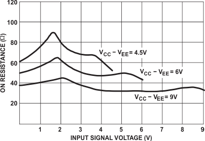
  Figure 5-3 Typical ON Resistance vs Input Signal Voltage
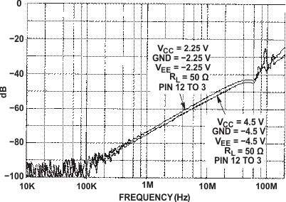
 Figure 5-5 Channel OFF Feedthrough (HC and HCT4051)
 Figure 5-2 Recommended Operating Area
as a Function of (VCC - GND).
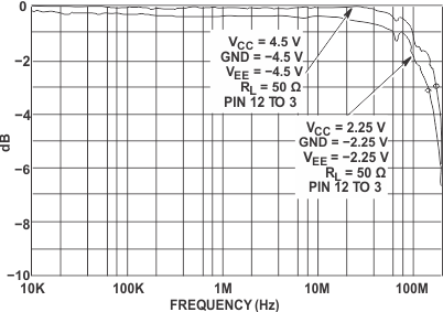
  Figure 5-4 Channel ON Bandwidth (HC and HCT4051)