SCAS945A June 2015 – September 2015 CDCEL824
PRODUCTION DATA.
- 1 Features
- 2 Applications
- 3 Description
- 4 Revision History
- 5 Description (continued)
- 6 Pin Configuration and Functions
- 7 Specifications
- 8 Parameter Measurement Information
- 9 Detailed Description
- 10Application and Implementation
- 11Power Supply Recommendations
- 12Layout
- 13Device and Documentation Support
- 14Mechanical, Packaging, and Orderable Information
Package Options
Mechanical Data (Package|Pins)
- PW|16
Thermal pad, mechanical data (Package|Pins)
Orderable Information
10 Application and Implementation
NOTE
Information in the following applications sections is not part of the TI component specification, and TI does not warrant its accuracy or completeness. TI’s customers are responsible for determining suitability of components for their purposes. Customers should validate and test their design implementation to confirm system functionality.
10.1 Application Information
CDCEL824 is an easy to use low-cost, programmable CMOS clock synthesizer. it can be used as a crystal buffer, clock synthesizer with separate output supply pin. CDCEL824 features on-chip loop filter. Programming can be done through SPI, pin-mode, or using on-chip EEPROM. This section shows some examples of using CDCEL824 in various applications.
10.2 Typical Application
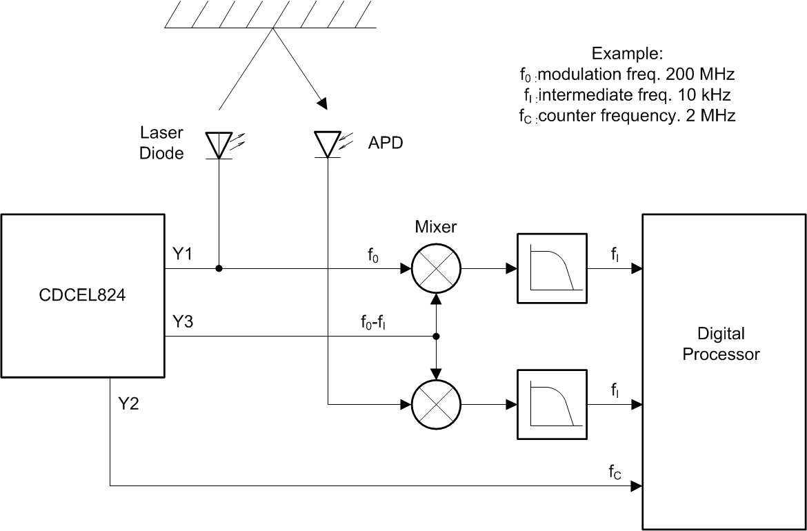
CDCEL824 is ideal clock generator for medium-range phase-shift laser distance meter. Having two separate PLLs allows for achieving as low intermediate frequency as required as well as high maximum modulation frequency, hence increasing the accuracy of the measurement device. Moreover, a fast settling PLL supports faster switching between multiple modulation frequencies required by a single measurement. this results in higher measurement rates for the device. Low power consumption and low cost position CDCEL824 as an ideal device for commercial laser distance metering equipment.
Figure 13 shows a typical application concept for the CDCEL824, where the outputs of the PLL1, Y1 and Y2 are used to generate the modulation and the counter frequency respectively. Y3 coming out of the PLL2 is carrying the shifted modulation frequency for down mixing. all three frequencies are programmable and dynamically switchable.
 Figure 13. Heterodyne Phase-Shift Laser Distance Meter Concept
10.2.1 Design Requirements
For Laser distance meter applications, if heterodyne technique is used as mentioned in Typical Application, it is shown that:


That means lower RF frequency allows for longer range, while lower ratio  ( higher RF frequency and lower IF frequency) gives lower error.
The values of intermediate, RF, and counter frequency should be chosen according to design targets of the maximum range and maximum tolerable error. Typically multiple consecutive measurements with multiple RF frequencies are carried on to resolve the trade-off between the accuracy and the maximum range.
10.2.2 Detailed Design Procedure
10.2.2.1 PLL Multiplier/Divider Definition
At a given input frequency (ƒIN), the output frequency (ƒOUT) of the CDCEL824 can be calculated:

where
- M (1 to 511) and N (1 to 4095) are the multiplier/divide values of the PLL
- Pdiv (1 to 127) is the output divider.
The target VCO frequency (ƒVCO) of each PLL can be calculated:

The PLL internally operates as fractional divider and needs the following multiplier/divider settings:
NP = 4 – int  Q = int
  R = N′ – M × Q
where
N′ = N × 2P
N ≥ M
80 MHz ≤ ƒVCO ≤ 200 MHz
16 ≤ q ≤ 63
0 ≤ p ≤ 4
0 ≤ r ≤ 511
| Example: | |||
| for ƒIN = 27 MHz; M = 1; N = 4; Pdiv = 2; | for ƒIN = 27 MHz; M = 2; N = 11; Pdiv = 2; | ||
| → | fOUT = 54 MHz | → | fOUT = 74.25 MHz |
| → | fVCO = 108 MHz | → | fVCO = 148.50 MHz |
| → | P = 4 – int(log24) = 4 – 2 = 2 | → | P = 4 – int(log25.5) = 4 – 2 = 2 |
| → | N′’ = 4 × 22 = 16 | → | N′’ = 11 × 22 = 44 |
| → | Q = int(16) = 16 | → | Q = int(22) = 22 |
| → | R = 16 – 16 = 0 | → | R = 44 – 44 = 0 |
The values for P, Q, R, and N’ are automatically calculated when using TI Pro-Clock™ software.
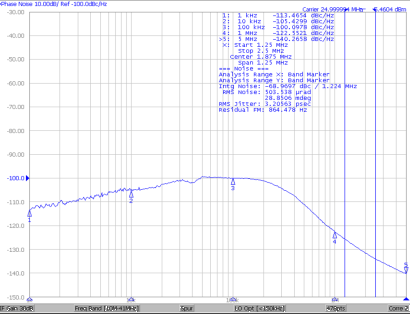
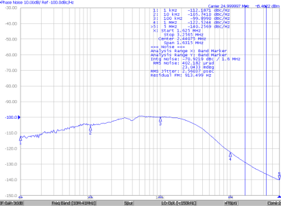
10.2.3 Application Curves

| 1.5 MHz to 2.5 MHz |

| 1.625 MHz to 3.25 MHz |