SCAS945A June   2015  – September 2015 CDCEL824

PRODUCTION DATA.  

  1. Features
  2. Applications
  3. Description
  4. Revision History
  5. Description (continued)
  6. Pin Configuration and Functions
  7. Specifications
    1. 7.1 Absolute Maximum Ratings
    2. 7.2 ESD Ratings
    3. 7.3 Recommended Operating Conditions
    4. 7.4 Thermal Information
    5. 7.5 Electrical Characteristics
    6. 7.6 CLK_IN Timing Requirements
    7. 7.7 SDA/SCL Timing Requirements
    8. 7.8 EEPROM Specification
    9. 7.9 Typical Characteristics
  8. Parameter Measurement Information
  9. Detailed Description
    1. 9.1 Overview
    2. 9.2 Functional Block Diagram
    3. 9.3 Feature Description
      1. 9.3.1 Control Pins Settings
      2. 9.3.2 SDA/SCL Serial Interface
      3. 9.3.3 SDA/SCL Hardware Interface
    4. 9.4 Device Functional Modes
      1. 9.4.1 Default Device Setting
    5. 9.5 Programming
      1. 9.5.1 Data Protocol
      2. 9.5.2 Command Code Definition
      3. 9.5.3 Generic Programming Sequence
      4. 9.5.4 Byte Write Programming Sequence
      5. 9.5.5 Byte Read Programming Sequence
      6. 9.5.6 Block Write Programming Sequence
      7. 9.5.7 Block Read Programming Sequence
    6. 9.6 Register Maps
      1. 9.6.1 SDA/SCL Configuration Registers
  10. 10Application and Implementation
    1. 10.1 Application Information
    2. 10.2 Typical Application
      1. 10.2.1 Design Requirements
      2. 10.2.2 Detailed Design Procedure
        1. 10.2.2.1 PLL Multiplier/Divider Definition
      3. 10.2.3 Application Curves
  11. 11Power Supply Recommendations
  12. 12Layout
    1. 12.1 Layout Guidelines
    2. 12.2 Layout Example
  13. 13Device and Documentation Support
    1. 13.1 Documentation Support
    2. 13.2 Community Resources
    3. 13.3 Trademarks
    4. 13.4 Electrostatic Discharge Caution
    5. 13.5 Glossary
  14. 14Mechanical, Packaging, and Orderable Information

Package Options

Mechanical Data (Package|Pins)
Thermal pad, mechanical data (Package|Pins)
Orderable Information

6 Pin Configuration and Functions

PW Package
20-Pin TSSOP
Top View
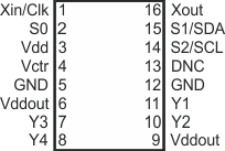
CDCEL824 Pinout_diagram_SCAS847.gif

Pin Functions

PIN I/O DESCRIPTION
NUMBER NAME
1 Xin/CLK I Crystal oscillator input or LVCMOS clock Input (selectable via SDA/SCL bus).
2 S0 I User-programmable control input S0; LVCMOS inputs; internal pullup.
3 VDD Power 1.8-V power supply for the device
4 VCtrl I VCXO control voltage (leave open or pull up when not used).
5, 12 GND Ground Ground
6, 9 VDDOUT Power 1.8-V supply for all outputs
7 Y3 O LVCMOS outputs
8 Y4 O LVCMOS outputs
10 Y2 O LVCMOS outputs
11 Y1 O LVCMOS outputs
13 DNC O Reserved pin, do not connect
14 SCL/S2 I SCL: Serial clock input (default configuration), LVCMOS; internal pullup.
S2: User-programmable control input; LVCMOS inputs; internal pullup.
15 SDA/S1 I/O or I SDA: Bidirectional serial data input/output (default configuration), LVCMOS; internal pullup
S1: User-programmable control input; LVCMOS inputs; internal pullup.
16 Xout O Crystal oscillator output (leave open or pull up when not used).