SNAS734F July 2017 – January 2024 CDCI6214
PRODUCTION DATA
- 1
- 1 Features
- 2 Applications
- 3 Description
- 4 Device Comparison
- 5 Pin Configuration and Functions
-
6 Specifications
- 6.1 Absolute Maximum Ratings
- 6.2 ESD Ratings
- 6.3 Recommended Operating Conditions
- 6.4 Thermal Information
- 6.5 EEPROM Characteristics
- 6.6 Reference Input, Single-Ended and Differential Mode Characteristics (REFP, REFN, FB_P, FB_N)
- 6.7 Reference Input, Crystal Mode Characteristics (XIN, XOUT)
- 6.8 General-Purpose Input and Output Characteristics (GPIO[4:1], SYNC/RESETN)
- 6.9 Triple Level Input Characteristics (EEPROMSEL, REFSEL)
- 6.10 Reference Mux Characteristics
- 6.11 Phase-Locked Loop Characteristics
- 6.12 Closed-Loop Output Jitter Characteristics
- 6.13 Output Mux Characteristics
- 6.14 LVCMOS Output Characteristics
- 6.15 HCSL Output Characteristics
- 6.16 LVDS DC-Coupled Output Characteristics
- 6.17 Programmable Differential AC-Coupled Output Characteristics
- 6.18 Output Skew and Delay Characteristics
- 6.19 Output Synchronization Characteristics
- 6.20 Timing Characteristics
- 6.21 I2C-Compatible Serial Interface Characteristics (SDA/GPIO2, SCL/GPIO3)
- 6.22 Timing Requirements, I2C-Compatible Serial Interface (SDA/GPIO2, SCL/GPIO3)
- 6.23 Power Supply Characteristics
- 6.24 Typical Characteristics
- 7 Parameter Measurement Information
-
8 Detailed Description
- 8.1 Overview
- 8.2 Functional Block Diagram
- 8.3 Feature Description
- 8.4 Device Functional Modes
- 8.5 Programming
- 9 Application and Implementation
- 10Register Maps
- 11Device and Documentation Support
- 12Revision History
- 13Mechanical, Packaging, and Orderable Information
Package Options
Refer to the PDF data sheet for device specific package drawings
Mechanical Data (Package|Pins)
- RGE|24
Thermal pad, mechanical data (Package|Pins)
Orderable Information
8.3.4.1 Global and Individual Output Enable: OE and OE_Y[4:1]
The output enable functionality allows to enable or disable all or a specific output buffer. The bypass copy on Y0 is excluded from the global output enable signal. When an output is disabled, it drives a configurable mute-state, ch[4:1]_mute-sel. When the serial interface is deactivated one can use all individual output enable signals at the same time, see mode. The individual output enable signal controls the respective output channel integer divider to gate the clock. Therefore each integer divider needs to be active. When multiple outputs are sourced from the same integer divider, the respective OE signal will enable/disable the output(s). (1)
When multiple output enable signals are configured on multiple-GPIO pins, then the global output enable OE has higher priority than the individual output enable OE[4:1]. An individual output enable OE[4:1] may only be configured on a single pin.
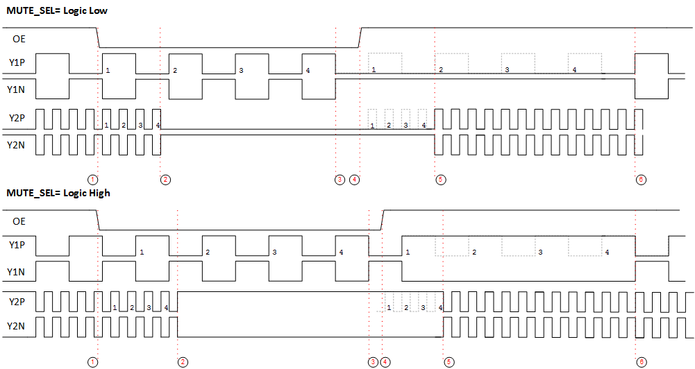
The individual output enable signal enables and disables the respective output in a deterministic way. Therefore the high and low level of the signal is qualified by counting four cycles of the respective output clock. The following steps can be seen in Figure 8-7:
- The OE falling edge which disables the outputs.
- Transition from logic high to logic low / logic low to logic high for Y2 after four rising edges.
- Transition from logic high to logic low / logic low to logic high for Y1 after four rising edges.
- The OE rising edge which enables the outputs.
- Output Y2 starts toggling after four rising edges.
- Output Y1 starts toggling after four rising edges.
 Figure 8-7 Individual Output Enable and Disable
The deterministic behaviour of the individual output enable is designed for an output frequency up to 200 MHz.