SNAS734F July   2017  – January 2024 CDCI6214

PRODUCTION DATA  

  1.   1
  2. Features
  3. Applications
  4. Description
  5. Device Comparison
  6. Pin Configuration and Functions
  7. Specifications
    1. 6.1  Absolute Maximum Ratings
    2. 6.2  ESD Ratings
    3. 6.3  Recommended Operating Conditions
    4. 6.4  Thermal Information
    5. 6.5  EEPROM Characteristics
    6. 6.6  Reference Input, Single-Ended and Differential Mode Characteristics (REFP, REFN, FB_P, FB_N)
    7. 6.7  Reference Input, Crystal Mode Characteristics (XIN, XOUT)
    8. 6.8  General-Purpose Input and Output Characteristics (GPIO[4:1], SYNC/RESETN)
    9. 6.9  Triple Level Input Characteristics (EEPROMSEL, REFSEL)
    10. 6.10 Reference Mux Characteristics
    11. 6.11 Phase-Locked Loop Characteristics
    12. 6.12 Closed-Loop Output Jitter Characteristics
    13. 6.13 Output Mux Characteristics
    14. 6.14 LVCMOS Output Characteristics
    15. 6.15 HCSL Output Characteristics
    16. 6.16 LVDS DC-Coupled Output Characteristics
    17. 6.17 Programmable Differential AC-Coupled Output Characteristics
    18. 6.18 Output Skew and Delay Characteristics
    19. 6.19 Output Synchronization Characteristics
    20. 6.20 Timing Characteristics
    21. 6.21 I2C-Compatible Serial Interface Characteristics (SDA/GPIO2, SCL/GPIO3)
    22. 6.22 Timing Requirements, I2C-Compatible Serial Interface (SDA/GPIO2, SCL/GPIO3)
    23. 6.23 Power Supply Characteristics
    24. 6.24 Typical Characteristics
  8. Parameter Measurement Information
    1. 7.1 Parameters
      1. 7.1.1 Reference Inputs
      2. 7.1.2 Outputs
      3. 7.1.3 Serial Interface
      4. 7.1.4 Power Supply
  9. Detailed Description
    1. 8.1 Overview
    2. 8.2 Functional Block Diagram
    3. 8.3 Feature Description
      1. 8.3.1 Reference Block
        1. 8.3.1.1 Input Stages
          1. 8.3.1.1.1 Crystal Oscillator
          2. 8.3.1.1.2 LVCMOS
          3. 8.3.1.1.3 Differential AC-Coupled
        2. 8.3.1.2 Reference Mux
        3. 8.3.1.3 Reference Divider
          1. 8.3.1.3.1 Doubler
        4. 8.3.1.4 Bypass-Mux
        5. 8.3.1.5 Zero Delay, Internal and External Path
      2. 8.3.2 Phase-Locked Loop
      3. 8.3.3 Clock Distribution
        1. 8.3.3.1 Output Channel
        2. 8.3.3.2 Divider Glitch-Less Update
      4. 8.3.4 Control Pins
        1. 8.3.4.1 Global and Individual Output Enable: OE and OE_Y[4:1]
      5. 8.3.5 Operation Modes
      6. 8.3.6 Divider Synchronization - SYNC
      7. 8.3.7 EEPROM - Cyclic Redundancy Check
      8. 8.3.8 Power Supplies
        1. 8.3.8.1 Power Management
    4. 8.4 Device Functional Modes
      1. 8.4.1 Pin Mode
      2. 8.4.2 Serial Interface Mode
        1. 8.4.2.1 Fall-Back Mode
    5. 8.5 Programming
      1. 8.5.1 Recommended Programming Procedure
      2. 8.5.2 EEPROM Access
      3. 8.5.3 Device Defaults
  10. Application and Implementation
    1. 9.1 Application Information
    2. 9.2 Typical Applications
      1. 9.2.1 Design Requirements
      2. 9.2.2 Detailed Design Procedure
      3. 9.2.3 Application Curves
    3. 9.3 Do's and Don'ts
    4. 9.4 Initialization Setup
    5. 9.5 Power Supply Recommendations
      1. 9.5.1 Power-Up Sequence
      2. 9.5.2 De-Coupling
    6. 9.6 Layout
      1. 9.6.1 Layout Guidelines
      2. 9.6.2 Layout Examples
  11. 10Register Maps
    1. 10.1 CDCI6214 Registers
    2. 10.2 EEPROM Map
  12. 11Device and Documentation Support
    1. 11.1 Device Support
      1. 11.1.1 Development Support
      2. 11.1.2 Device Nomenclature
    2. 11.2 Receiving Notification of Documentation Updates
    3. 11.3 Support Resources
    4. 11.4 Trademarks
    5. 11.5 Electrostatic Discharge Caution
    6. 11.6 Glossary
  13. 12Revision History
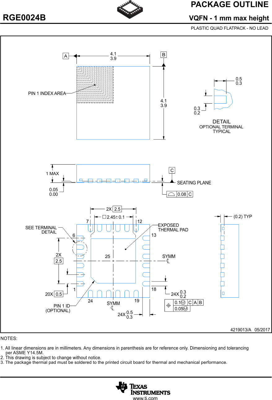
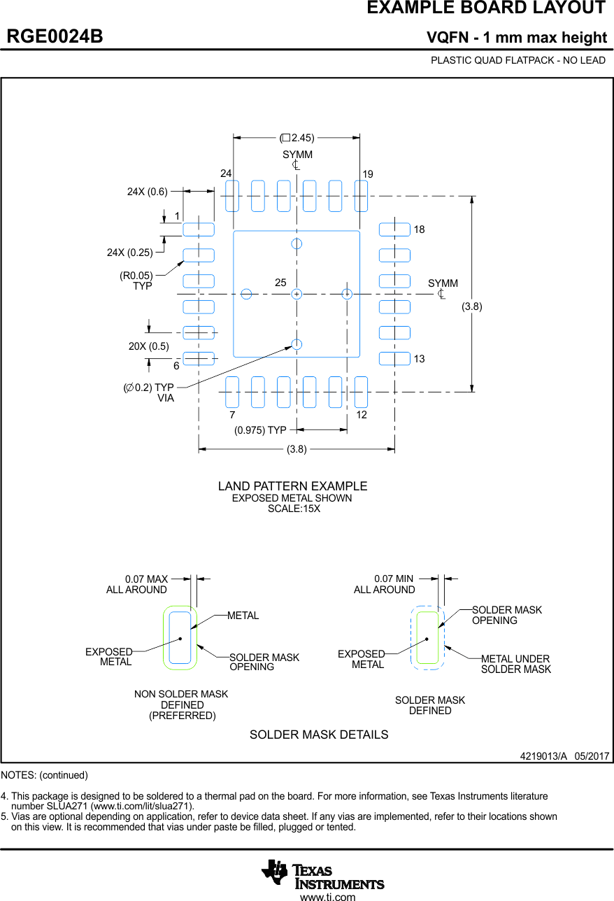
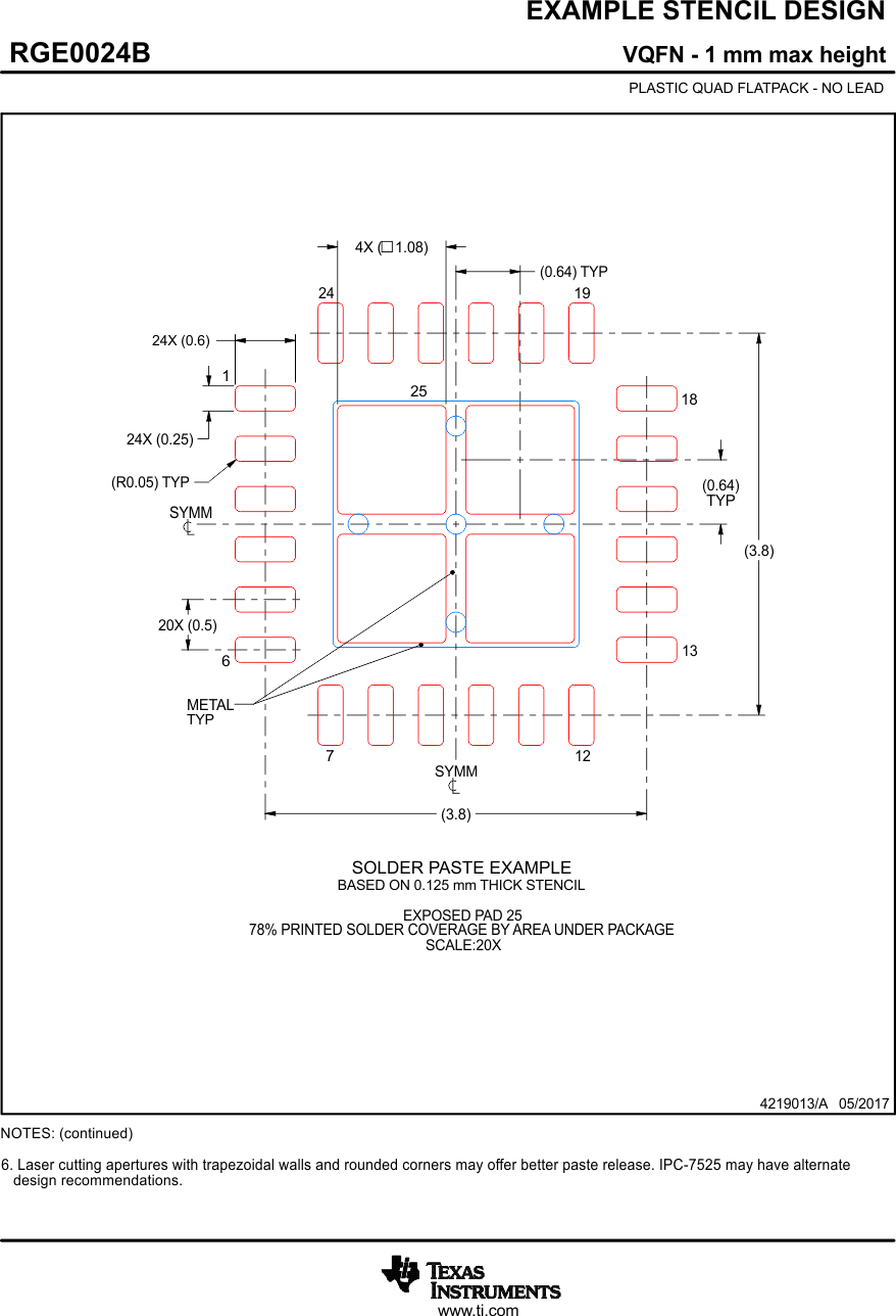
  14. 13Mechanical, Packaging, and Orderable Information

Package Options

Refer to the PDF data sheet for device specific package drawings

Mechanical Data (Package|Pins)
  • RGE|24
Thermal pad, mechanical data (Package|Pins)
Orderable Information

Mechanical, Packaging, and Orderable Information

The following pages include mechanical, packaging, and orderable information. This information is the most current data available for the designated devices. This data is subject to change without notice and revision of this document. For browser-based versions of this data sheet, refer to the left-hand navigation.

GUID-1C98053E-9760-4A48-AC13-FF3647C9B769-low.gif
GUID-9FA1D935-CF85-44CA-BE93-0D100B66C753-low.gif
GUID-FF0F1DB0-BD72-494E-B9B8-22404D84A346-low.gif