SCAS666D June 2001 – October 2015 CDCVF2310
PRODUCTION DATA.
- 1 Features
- 2 Applications
- 3 Description
- 4 Revision History
- 5 Pin Configuration and Functions
- 6 Specifications
- 7 Parameter Measurement Information
- 8 Detailed Description
- 9 Application and Implementation
- 10Power Supply Recommendations
- 11Layout
- 12Device and Documentation Support
- 13Mechanical, Packaging, and Orderable Information
Package Options
Refer to the PDF data sheet for device specific package drawings
Mechanical Data (Package|Pins)
- PW|24
Thermal pad, mechanical data (Package|Pins)
Orderable Information
8 Detailed Description
8.1 Overview
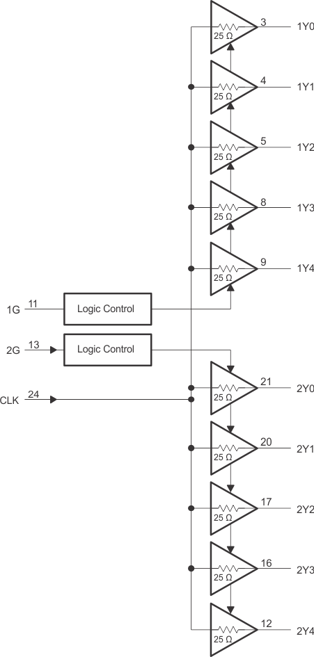
The CDCVF2310 is a high-performance, low-skew clock buffer that operates up to 200 MHz. Two banks of five outputs each provide low-skew copies of CLK. After power up, the default state of the outputs is low regardless of the state of the control pins. For normal operation, the outputs of bank 1Y[0:4] or 2Y[0:4] can be placed in a low state when the control pins (1G or 2G, respectively) are held low and a negative clock edge is detected on the CLK input. The outputs of bank 1Y[0:4] or 2Y[0:4] can be switched into the buffer mode when the control pins (1G and 2G) are held high and a negative clock edge is detected on the CLK input. The device operates in a 2.5-V and 3.3-V environment. The built-in output enable glitch suppression ensures a synchronized output enable sequence to distribute full period clock signals.
8.2 Functional Block Diagram

8.3 Feature Description
8.3.1 Output Enable Glitch Suppression Circuit
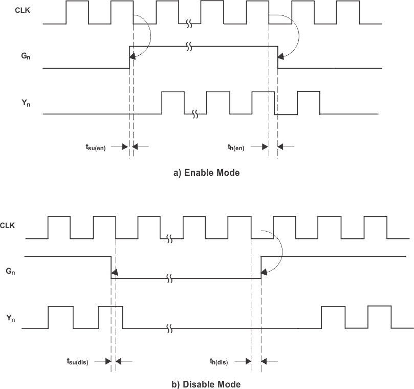
The purpose of the glitch suppression circuitry is to ensure the output enable sequence is synchronized with the clock input such that the output buffer is enabled or disabled on the next full period of the input clock (negative edge triggered by the input clock) (see Figure 6).
The G input must fulfill the timing requirements (tsu, th) according to the Switching Characteristics table for predictable operation.
 Figure 6. Enable and Disable Mode Relative to CLK↓
8.4 Device Functional Modes
Table 1 lists the functional modes for the CDCVF2310.