SCAS666D June 2001 – October 2015 CDCVF2310
PRODUCTION DATA.
- 1 Features
- 2 Applications
- 3 Description
- 4 Revision History
- 5 Pin Configuration and Functions
- 6 Specifications
- 7 Parameter Measurement Information
- 8 Detailed Description
- 9 Application and Implementation
- 10Power Supply Recommendations
- 11Layout
- 12Device and Documentation Support
- 13Mechanical, Packaging, and Orderable Information
Package Options
Refer to the PDF data sheet for device specific package drawings
Mechanical Data (Package|Pins)
- PW|24
Thermal pad, mechanical data (Package|Pins)
Orderable Information
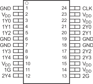
5 Pin Configuration and Functions
PW Package
24-Pin TSSOP
Top View

Pin Functions
| PIN | I/O | DESCRIPTION | |
|---|---|---|---|
| NAME | NO. | ||
| 1G | 11 | I | Output enable control for 1Y[0:4] outputs. This output enable is active-high, meaning the 1Y[0:4] clock outputs follow the input clock (CLK) if this pin is logic high. |
| 2G | 13 | I | Output enable control for 2Y[0:4] outputs. This output enable is active-high, meaning the 2Y[0:4] clock outputs follow the input clock (CLK) if this pin is logic high. |
| 1Y[0:4] | 3, 4, 5, 8, 9 | O | Buffered output clocks |
| 2Y[0:4] | 21, 20, 17, 16, 12 | O | Buffered output clocks |
| CLK | 24 | I | Input reference frequency |
| GND | 1, 6, 7, 18, 19 | — | Ground |
| VDD | 2, 10, 14, 15, 22, 23 | — | DC power supply, 2.3 V – 3.6 V |