SLPS411G April 2013 – January 2022 CSD17381F4
PRODUCTION DATA
- 1Features
- 2Applications
- 3Description
- 4Revision History
- 5Specifications
- 6Device and Documentation Support
- 7Mechanical, Packaging, and Orderable Information
Package Options
Refer to the PDF data sheet for device specific package drawings
Mechanical Data (Package|Pins)
- YJC|3
Thermal pad, mechanical data (Package|Pins)
Orderable Information
7.1 Mechanical Dimensions
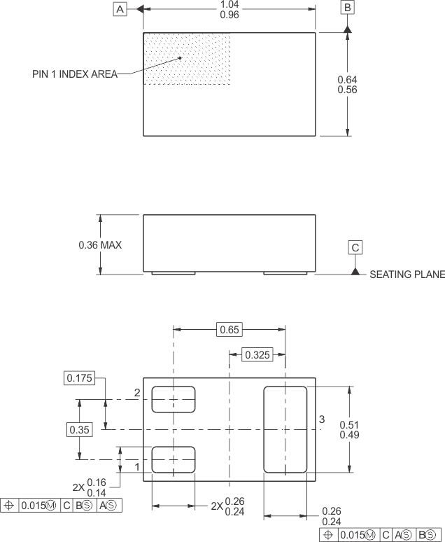
All linear dimensions are in
millimeters. Any dimensions in parenthesis are for reference only. Dimensioning
and tolerancing per ASME Y14.5M.
This drawing is subject to change
without notice.
This package is a Pb-free bump
design. Bump finish may vary. To determine the exact finish, refer to the device
data sheet or contact a local TI representative.