SLPS350A February 2014 – January 2017 CSD87333Q3D
PRODUCTION DATA.
- 1 Features
- 2 Applications
- 3 Description
- 4 Revision History
- 5 Specifications
- 6 Applications
- 7 Recommended PCB Design Overview
- 8 Thermal Performance
- 9 Device and Documentation Support
- 10Mechanical, Packaging, and Orderable Information
Package Options
Mechanical Data (Package|Pins)
- DPB|8
Thermal pad, mechanical data (Package|Pins)
Orderable Information
1 Features
- Half-Bridge Power Block
- Optimized for High-Duty Cycle
- Up to 24 Vin
- 94.7% System Efficiency at 8 A
- 1.5 W PLoss at 8 A
- Up to 15-A Operation
- High-Frequency Operation (up to 1.5 MHz)
- High-Density SON 3.3-mm × 3.3-mm Footprint
- Optimized for 5-V Gate Drive
- Low-Switching Losses
- Ultra-Low Inductance Package
- RoHS Compliant
- Halogen Free
- Lead-Free Terminal Plating
2 Applications
- Synchronous Buck Converters
- High-Frequency Applications
- High-Duty Cycle Applications
- Synchronous Boost Converters
- POL DC-DC Converters
3 Description
The CSD87333Q3D NexFET™ power block is an optimized design for synchronous buck and boost applications offering high-current, high-efficiency, and high-frequency capability in a small 3.3-mm × 3.3-mm outline. Optimized for 5-V gate drive applications, this product offers a flexible solution in high-duty cycle applications when paired with an external controller or driver.
.
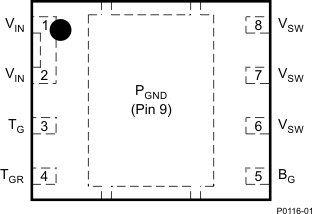
Top View

Device Information(1)
| DEVICE | MEDIA | QTY | PACKAGE | SHIP |
|---|---|---|---|---|
| CSD87333Q3D | 13-Inch Reel | 2500 | SON 3.30-mm × 3.30-mm Plastic Package |
Tape and Reel |
| CSD87333Q3DT | 7-Inch Reel | 250 |
- For all available packages, see the orderable addendum at the end of the data sheet.
.
.
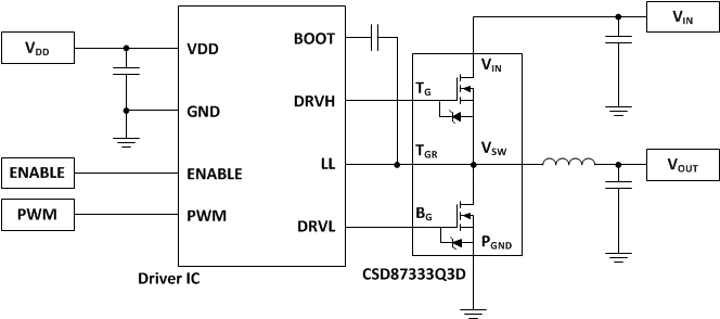
Typical Circuit

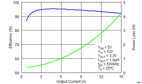
Typical Power Block Efficiency and Power Loss
