SLPS430A August 2013 – August 2014 CSD95375Q4M
PRODUCTION DATA.
- 1 Features
- 2 Applications
- 3 Description
- 4 Revision History
- 5 Pin Configuration
- 6 Specifications
- 7 Electrical Characteristics
- 8 Typical Characteristics
- 9 Detailed Description
- 10Application and Implementation
- 11Layout
- 12Device and Documentation Support
- 13Mechanical, Packaging, and Orderable Information
Package Options
Mechanical Data (Package|Pins)
- DPC|8
Thermal pad, mechanical data (Package|Pins)
Orderable Information
9 Detailed Description
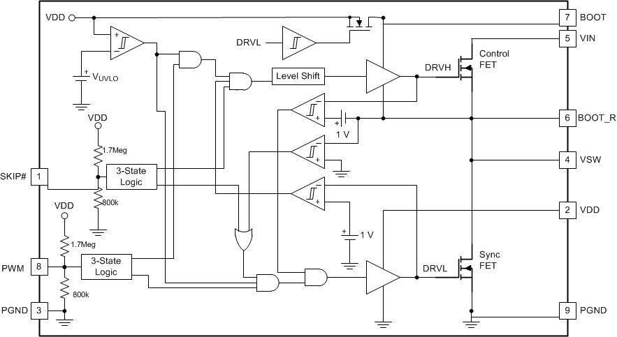
9.1 Functional Block Diagram
9.2 Feature Description
9.2.1 Powering CSD95375Q4M And Gate Drivers
An external VDD voltage is required to supply the integrated gate driver IC and provide the necessary gate drive power for the MOSFETS. A 1 µF 10 V X5R or higher ceramic capacitor is recommended to bypass VDD pin to PGND. A bootstrap circuit to provide gate drive power for the Control FET is also included. The bootstrap supply to drive the Control FET is generated by connecting a 100 nF 16 V X5R ceramic capacitor between BOOT and BOOT_R pins. An optional RBOOT resistor can be used to slow down the turn on speed of the Control FET and reduce voltage spikes on the VSW node. A typical 1 Ω to 4.7 Ω value is a compromise between switching loss and VSW spike amplitude.
9.3 Undervoltage Lockout Protection (UVLO)
The undervoltage lockout (UVLO) comparator evaluates the VDD voltage level. As VVDD rises, both the Control FET and Sync FET gates hold actively low at all times until VVDD reaches the higher UVLO threshold (VUVLO_H)., Then the driver becomes operational and responds to PWM and SKIP# commands. If VDD falls below the lower UVLO threshold (VUVLO_L = VUVLO_H – Hysteresis), the device disables the driver and drives the outputs of the Control FET and Sync FET gates actively low. Figure 12 shows this function.
CAUTION
Do not start the driver in the very low power mode (SKIP# = Tri-state).
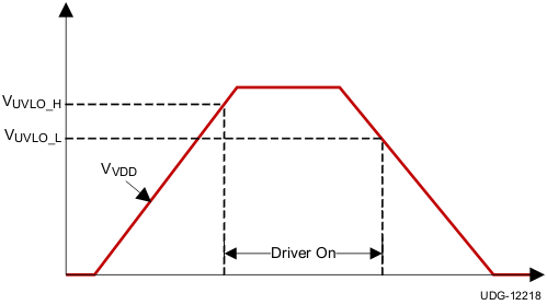 Figure 12. UVLO Operation
9.4 PWM Pin
The PWM pin incorporates an input tri-state function. The device forces the gate driver outputs to low when PWM is driven into the tri-state window and the driver enters a low power state with zero exit latency. The pin incorporates a weak pull-up to maintain the voltage within the tri-state window during low-power modes. Operation into and out of tri-state mode follows the timing diagram outlined in Figure 13.
When VDD reaches the UVLO_H level, a tri-state voltage range (window) is set for the PWM input voltage. The window is defined the PWM voltage range between PWM logic high (VIH) and logic low (VIL) thresholds. The device sets high-level input voltage and low-level input voltage threshold levels to accommodate both 3.3 V (typical) and 5 V (typical) PWM drive signals.
When the PWM exits tri-state, the driver enters CCM for a period of 4 µs, regardless of the state of the SKIP# pin. Normal operation requires this time period in order for the auto-zero comparator to resume.
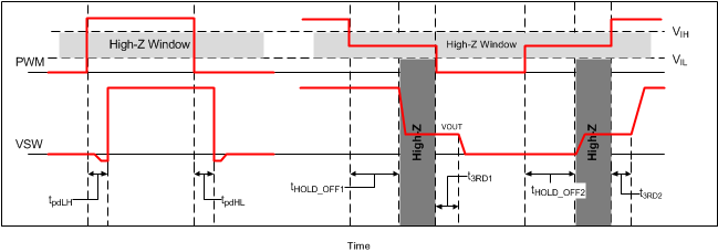 Figure 13. PWM Tri-State Timing Diagram
9.5 SKIP# Pin
The SKIP# pin incorporates the input tri-state buffer as PWM. The function is somewhat different. When SKIP# is low, the zero crossing (ZX) detection comparator is enabled, and DCM mode operation occurs if the load current is less than the critical current. When SKIP# is high, the ZX comparator disables, and the converter enters FCCM mode. When both SKIP# and PWM are tri-stated, normal operation forces the gate driver outputs low and the driver enters a low-power state. In the low-power state, the UVLO comparator remains off to reduce quiescent current. When SKIP# is pulled low, the driver wakes up and is able to accept PWM pulses in less than 50 µs.
Table 1 shows the logic functions of UVLO, PWM, SKIP#, the Control FET Gate and the Sync FET Gate.
Table 1. Logic Functions of the Driver IC
| UVLO | PWM | SKIP# | Sync FET Gate | Control FET Gate | MODE |
|---|---|---|---|---|---|
| Active | — | — | Low | Low | Disabled |
| Inactive | Low | Low | High(1) | Low | DCM(1) |
| Inactive | Low | High | High | Low | FCCM |
| Inactive | High | H or L | Low | High | — |
| Inactive | Tri-state | H or L | Low | Low | LQ |
| Inactive | — | Tri-state | Low | Low | ULQ |
9.5.1 Zero Crossing (ZX) Operation
The zero crossing comparator is adaptive for improved accuracy. As the output current decreases from a heavy load condition, the inductor current also reduces and eventually arrives at a valley, where it touches zero current, which is the boundary between continuous conduction and discontinuous conduction modes. The SW pin detects the zero-current condition. When this zero inductor current condition occurs, the ZX comparator turns off the rectifying MOSFET.
9.6 Integrated Boost-Switch
To maintain a BST-SW voltage close to VDD (to get lower conduction losses on the high-side FET), the conventional diode between the VDD pin and the BST pin is replaced by a FET which is gated by the DRVL signal.