SLPS430A August 2013 – August 2014 CSD95375Q4M
PRODUCTION DATA.
- 1 Features
- 2 Applications
- 3 Description
- 4 Revision History
- 5 Pin Configuration
- 6 Specifications
- 7 Electrical Characteristics
- 8 Typical Characteristics
- 9 Detailed Description
- 10Application and Implementation
- 11Layout
- 12Device and Documentation Support
- 13Mechanical, Packaging, and Orderable Information
Package Options
Mechanical Data (Package|Pins)
- DPC|8
Thermal pad, mechanical data (Package|Pins)
Orderable Information
11 Layout
11.1 Layout Guidelines
11.1.1 Recommended PCB Design Overview
There are two key system-level parameters that can be addressed with a proper PCB design: electrical and thermal performance. Properly optimizing the PCB layout will yield maximum performance in both areas. Below is a brief description on how to address each parameter.
11.1.2 Electrical Performance
The CSD95375Q4M has the ability to switch at voltage rates greater than 10 kV/µs. Special care must be then taken with the PCB layout design and placement of the input capacitors, inductor and output capacitors.
- The placement of the input capacitors relative to VIN and PGND pins of CSD95375Q4M device should have the highest priority during the component placement routine. It is critical to minimize these node lengths. As such, ceramic input capacitors need to be placed as close as possible to the VIN and PGND pins (see Figure 16). The example in Figure 16 uses 1 × 1 nF 0402 25 V and 3 × 10 µF 1206 25 V ceramic capacitors (TDK Part # C3216X5R1C106KT or equivalent). Notice there are ceramic capacitors on both sides of the board with an appropriate amount of vias interconnecting both layers. In terms of priority of placement next to the Power Stage C5, C8 and C6, C19 should follow in order.
- The bootstrap cap CBOOT 0.1 µF 0603 16 V ceramic capacitor should be closely connected between BOOT and BOOT_R pins
- The switching node of the output inductor should be placed relatively close to the Power Stage CSD95375Q4M VSW pins. Minimizing the VSW node length between these two components will reduce the PCB conduction losses and actually reduce the switching noise level. (1)
11.1.3 Thermal Performance
The CSD95375Q4M has the ability to use the GND planes as the primary thermal path. As such, the use of thermal vias is an effective way to pull away heat from the device and into the system board. Concerns of solder voids and manufacturability problems can be addressed by the use of three basic tactics to minimize the amount of solder attach that will wick down the via barrel:
- Intentionally space out the vias from each other to avoid a cluster of holes in a given area.
- Use the smallest drill size allowed in your design. The example in Figure 16 uses vias with a 10 mil drill hole and a 16 mil capture pad.
- Tent the opposite side of the via with solder-mask.
In the end, the number and drill size of the thermal vias should align with the end user’s PCB design rules and manufacturing capabilities.
11.2 Layout Example
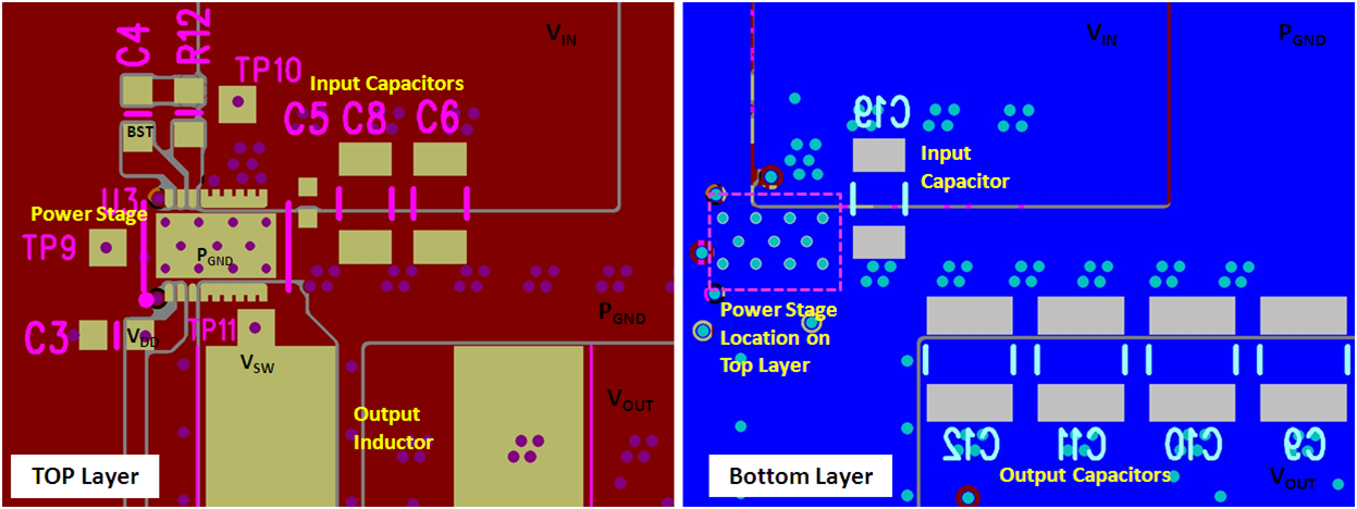 Figure 16. Recommended PCB Layout (Top Down View)