SLPS430A August   2013  – August 2014 CSD95375Q4M

PRODUCTION DATA.  

  1. Features
  2. Applications
  3. Description
  4. Revision History
  5. Pin Configuration
  6. Specifications
    1. 6.1 Absolute Maximum Ratings
    2. 6.2 Recommended Operating Conditions
    3. 6.3 Thermal Information
  7. Electrical Characteristics
  8. Typical Characteristics
  9. Detailed Description
    1. 9.1 Functional Block Diagram
    2. 9.2 Feature Description
      1. 9.2.1 Powering CSD95375Q4M And Gate Drivers
    3. 9.3 Undervoltage Lockout Protection (UVLO)
    4. 9.4 PWM Pin
    5. 9.5 SKIP# Pin
      1. 9.5.1 Zero Crossing (ZX) Operation
    6. 9.6 Integrated Boost-Switch
  10. 10Application and Implementation
    1. 10.1 Application Information
      1. 10.1.1 Power Loss Curves
      2. 10.1.2 Safe Operating Curves (SOA)
      3. 10.1.3 Normalized Curves
      4. 10.1.4 Calculating Power Loss and SOA
        1. 10.1.4.1 Design Example
        2. 10.1.4.2 Calculating Power Loss
        3. 10.1.4.3 Calculating SOA Adjustments
  11. 11Layout
    1. 11.1 Layout Guidelines
      1. 11.1.1 Recommended PCB Design Overview
      2. 11.1.2 Electrical Performance
      3. 11.1.3 Thermal Performance
    2. 11.2 Layout Example
  12. 12Device and Documentation Support
    1. 12.1 Trademarks
    2. 12.2 Electrostatic Discharge Caution
    3. 12.3 Glossary
  13. 13Mechanical, Packaging, and Orderable Information
    1. 13.1 Mechanical Drawing
    2. 13.2 Recommended PCB Land Pattern
    3. 13.3 Recommended Stencil Opening

Package Options

Mechanical Data (Package|Pins)
  • DPC|8
Thermal pad, mechanical data (Package|Pins)
Orderable Information

8 Typical Characteristics

TJ = 125°C, unless stated otherwise.
graph01_SLPS430.png
Figure 2. Power Loss vs Output Current
graph03_SLPS430.png
Figure 4. Safe Operating Area (SOA) – PCB Horizontal Mount (1)
graph05p2_SLPS430.png
Figure 6. Normalized Power Loss vs Frequency
graph07p2_SLPS430.png
Figure 8. Normalized Power Loss vs Output Voltage
graph09_SLPS430.png
Figure 10. Driver Current vs Frequency
graph02_SLPS430.png
Figure 3. Power Loss vs Temperature
graph04P2_SLPS430.png
Figure 5. Typical Safe Operating Area (SOA) (1)
graph06_SLPS430.png
Figure 7. Normalized Power Loss vs Input Voltage
graph08_SLPS430.png
Figure 9. Normalized Power Loss vs Output Inductance
graph10_SLPS430.png
Figure 11. Driver Current vs Temperature
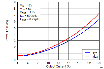
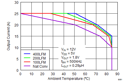
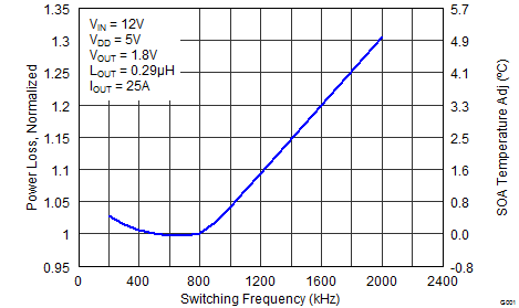
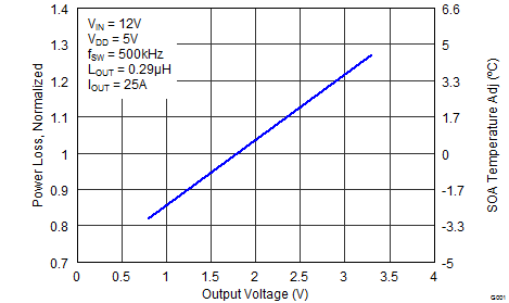
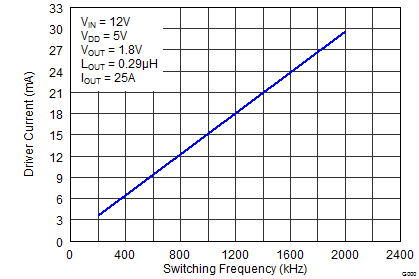
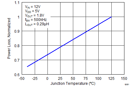
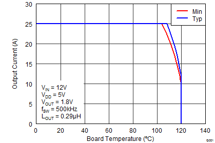
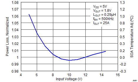
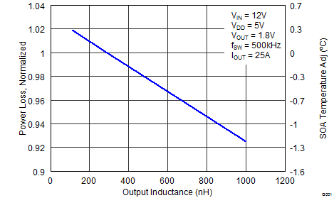
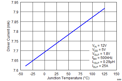
  1. The Typical CSD95375Q4M System Characteristic curves are based on measurements made on a PCB design with dimensions of 4" (W) × 3.5" (L) × 0.062" (T) and 6 copper layers of 1 oz. copper thickness. See the Application Information section for detailed explanation.