SLPS382D January   2013  – August 2016 CSD97374Q4M


  1. Features
  2. Applications
  3. Description
  4. Revision History
  5. Pin Configuration and Functions
  6. Specifications
    1. 6.1 Absolute Maximum Ratings
    2. 6.2 ESD Ratings
    3. 6.3 Recommended Operating Conditions
    4. 6.4 Thermal Information
    5. 6.5 Electrical Characteristics
    6. 6.6 Typical Characteristics
  7. Detailed Description
    1. 7.1 Functional Block Diagram
    2. 7.2 Powering CSD97374Q4M and Gate Drivers
    3. 7.3 Undervoltage Lockout Protection (UVLO)
    4. 7.4 PWM Pin
    5. 7.5 SKIP# Pin
      1. 7.5.1 Zero Crossing (ZX) Operation
    6. 7.6 Integrated Boost-Switch
  8. Application and Implementation
    1. 8.1 Application Information
    2. 8.2 Power Loss Curves
    3. 8.3 Safe Operating Curves (SOA)
    4. 8.4 Normalized Curves
    5. 8.5 Calculating Power Loss and SOA
      1. 8.5.1 Design Example
      2. 8.5.2 Calculating Power Loss
      3. 8.5.3 Calculating SOA Adjustments
  9. Layout
    1. 9.1 Layout Guidelines
      1. 9.1.1 Recommended PCB Design Overview
      2. 9.1.2 Electrical Performance
      3. 9.1.3 Thermal Performance
    2. 9.2 Layout Example
  10. 10Device and Documentation Support
    1. 10.1 Receiving Notification of Documentation Updates
    2. 10.2 Community Resources
    3. 10.3 Trademarks
    4. 10.4 Electrostatic Discharge Caution
    5. 10.5 Glossary
  11. 11Mechanical, Packaging, and Orderable Information
    1. 11.1 Recommended PCB Land Pattern
    2. 11.2 Recommended Stencil Opening

Package Options

Mechanical Data (Package|Pins)
  • DPC|8
Thermal pad, mechanical data (Package|Pins)
Orderable Information

11 Mechanical, Packaging, and Orderable Information

The following pages include mechanical, packaging, and orderable information. This information is the most current data available for the designated devices. This data is subject to change without notice and revision of this document. For browser-based versions of this data sheet, refer to the left-hand navigation.
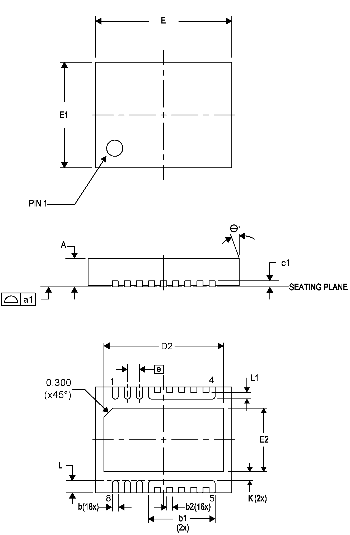
CSD97374Q4M Mechanical_Drawing0513.png
DIM MILLIMETERS INCHES
MIN NOM MAX MIN NOM MAX
A 0.800 0.900 1.000 0.031 0.035 0.039
a1 0.000 0.000 0.080 0.000 0.000 0.003
b 0.150 0.200 0.250 0.006 0.008 0.010
b1 2.000 2.200 2.400 0.079 0.087 0.095
b2 0.150 0.200 0.250 0.006 0.008 0.010
c1 0.150 0.200 0.250 0.006 0.008 0.010
D2 3.850 3.950 4.050 0.152 0.156 0.160
E 4.400 4.500 4.600 0.173 0.177 0.181
E1 3.400 3.500 3.600 0.134 0.138 0.142
E2 2.000 2.100 2.200 0.079 0.083 0.087
e 0.400 TYP 0.016 TYP
K 0.300 TYP 0.012 TYP
L 0.300 0.400 0.500 0.012 0.016 0.020
L1 0.180 0.230 0.280 0.007 0.009 0.011
θ 0.00 0.00

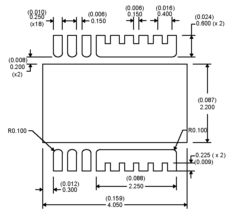
11.1 Recommended PCB Land Pattern

CSD97374Q4M PCB0513.png

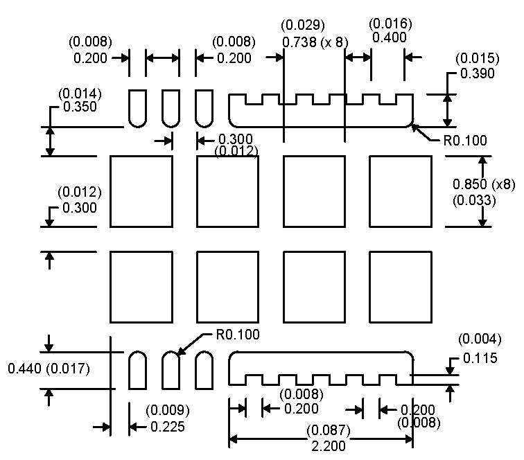
11.2 Recommended Stencil Opening

CSD97374Q4M Stencil0513.png

NOTE:

Dimensions are in mm (inches).