SLASEL0B October   2019  – June 2020 DAC11001A , DAC81001 , DAC91001

PRODUCTION DATA.  

  1. Features
  2. Applications
  3. Description
    1.     Device Images
      1.      Functional Block Diagram
      2.      High-Precision, Control-Loop Circuit
  4. Revision History
  5. Device Comparison Table
  6. Pin Configuration and Functions
    1.     Pin Functions
  7. Specifications
    1. 7.1      Absolute Maximum Ratings
    2. 7.2      ESD Ratings
    3. 7.3      Recommended Operating Conditions
    4. 7.4      Thermal Information Package
    5. 7.5      Electrical Characteristics
    6. Table 1. Timing Requirements: Write, 4.5 V ≤ DVDD ≤ 5.5 V
    7. Table 2. Timing Requirements: Write, 2.7 V ≤ DVDD < 4.5 V
    8. Table 3. Timing Requirements: Read and Daisy-Chain Write, 4.5 V ≤ DVDD ≤ 5.5 V
    9. Table 4. Timing Requirements: Read and Daisy-Chain Write, 2.7 V ≤ DVDD < 4.5 V
    10. 7.6      Typical Characteristics
  8. Detailed Description
    1. 8.1 Overview
    2. 8.2 Functional Block Diagram
    3. 8.3 Feature Description
      1. 8.3.1 Digital-to-Analog Converter Architecture
      2. 8.3.2 External Reference
      3. 8.3.3 Output Buffers
      4. 8.3.4 Internal Power-On Reset (POR)
      5. 8.3.5 Temperature Drift and Calibration
      6. 8.3.6 DAC Output Deglitch Circuit
    4. 8.4 Device Functional Modes
      1. 8.4.1 Fast-Settling Mode and THD
      2. 8.4.2 DAC Update Rate Mode
    5. 8.5 Programming
      1. 8.5.1 Daisy-Chain Operation
      2. 8.5.2 CLR Pin Functionality and Software Clear
      3. 8.5.3 Output Update (Synchronous and Asynchronous)
        1. 8.5.3.1 Synchronous Update
        2. 8.5.3.2 Asynchronous Update
      4. 8.5.4 Software Reset Mode
    6. 8.6 Register Map
      1. 8.6.1 NOP Register (address = 00h) [reset = 0x000000h]
        1. Table 9. NOP Register Field Descriptions
      2. 8.6.2 DAC-DATA Register (address = 01h) [reset = 0x000000h]
        1. Table 10. DAC-DATA Register Field Descriptions
      3. 8.6.3 CONFIG1 Register (address = 02h) [reset = 004C80h for bits [23:0]]
        1. Table 11. CONFIG1 Register Field Descriptions
      4. 8.6.4 DAC-CLEAR-DATA Register (address = 03h) [reset = 000000h for bits [23:0]]
        1. Table 12. DAC-CLEAR-DATA Register Field Descriptions
      5. 8.6.5 TRIGGER Register (address = 04h) [reset = 000000h for bits [23:0]]
        1. Table 13. TRIGGER Register Field Descriptions
      6. 8.6.6 STATUS Register (address = 05h) [reset = 000000h for bits [23:0]]
        1. Table 14. STATUS Register Field Descriptions
      7. 8.6.7 CONFIG2 Register (address = 06h) [reset = 000040h for bits [23:0]]
        1. Table 15. CONFIG2 Register Field Descriptions
  9. Application and Implementation
    1. 9.1 Application Information
    2. 9.2 Typical Application
      1. 9.2.1 Source Measure Unit (SMU)
        1. 9.2.1.1 Design Requirements
        2. 9.2.1.2 Detailed Design Procedure
        3. 9.2.1.3 Application Curves
      2. 9.2.2 Battery Test Equipment (BTE)
        1. 9.2.2.1 Design Requirements
        2. 9.2.2.2 Detailed Design Procedure
        3. 9.2.2.3 Application Curves
      3. 9.2.3 High-Precision Control Loop
        1. 9.2.3.1 Design Requirements
        2. 9.2.3.2 Detailed Design Procedure
        3. 9.2.3.3 Application Curves
      4. 9.2.4 Arbitrary Waveform Generation (AWG)
        1. 9.2.4.1 Design Requirements
        2. 9.2.4.2 Detailed Design Procedure
        3. 9.2.4.3 Application Curves
    3. 9.3 System Examples
      1. 9.3.1 Interfacing to a Processor
      2. 9.3.2 Interfacing to a Low-Jitter LDAC Source
      3. 9.3.3 Embedded Resistor Configurations
        1. 9.3.3.1 Minimizing Bias Current Mismatch
        2. 9.3.3.2 2x Gain configuration
        3. 9.3.3.3 Generating Negative Reference
    4. 9.4 What to Do and What Not to Do
      1. 9.4.1 What to Do
      2. 9.4.2 What Not to Do
    5. 9.5 Initialization Set Up
  10. 10Power Supply Recommendations
    1. 10.1 Power-Supply Sequencing
  11. 11Layout
    1. 11.1 Layout Guidelines
    2. 11.2 Layout Example
  12. 12Device and Documentation Support
    1. 12.1 Device Support
      1. 12.1.1 Development Support
    2. 12.2 Documentation Support
      1. 12.2.1 Related Documentation
    3. 12.3 Related Links
    4. 12.4 Receiving Notification of Documentation Updates
    5. 12.5 Support Resources
    6. 12.6 Trademarks
    7. 12.7 Electrostatic Discharge Caution
    8. 12.8 Glossary
  13. 13Mechanical, Packaging, and Orderable Information

Package Options

Mechanical Data (Package|Pins)
Thermal pad, mechanical data (Package|Pins)
Orderable Information

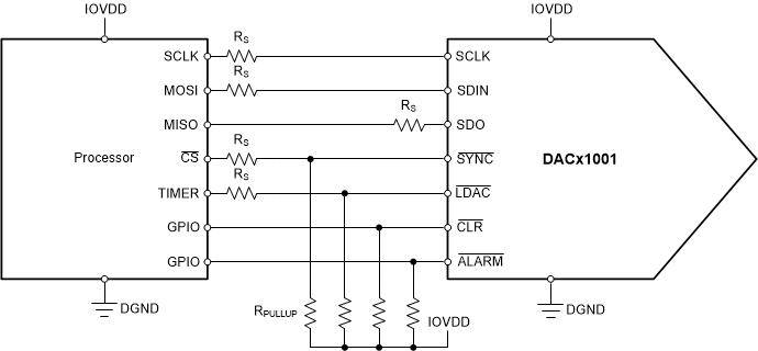
Interfacing to a Processor

The DACx1001 family of DACs works with a 4-wire SPI interface. The digital interface of the DACx1001 to a processor is shown in Figure 67. The DACx1001 has an LDAC input option for synchronous output update. In ac-signal generation applications, the jitter in the LDAC signal contributes to signal-to-noise ratio (SNR). Therefore, the LDAC signal must be generated from a low-jitter timer in the processor. The CLR and ALARM pins are static signals, and therefore can be connected to general-purpose input-output (GPIO) pins on the processor. All active-low signals (SYNC, LDAC, CLR, and ALARM) must be pulled up to IOVDD using 10-kΩ resistors. ALARM is an output pin from the DAC, so the corresponding GPIO on the processor must be configured as an input. Either poll the GPIO, or configured the GPIO as an interrupt to detect any failure alarm from the DAC. When using a high SCLK frequency, use source termination resistors, as shown in Interfacing to a Processor. Typically, 33-Ω resistors work on printed circuit boards (PCBs) with a 50-Ω trace impedance.
DAC11001A DAC91001 DAC81001 dac11001-interfacing-to-processor.gifFigure 67. Interfacing to a Processor