SBAS334D November 2004 – July 2016 DAC5675A
PRODUCTION DATA.
- 1 Features
- 2 Applications
- 3 Description
- 4 Revision History
- 5 Description Continued
- 6 Pin Configuration and Functions
- 7 Specifications
- 8 Detailed Description
- 9 Application and Implementation
- 10Power Supply Recommendations
- 11Layout
- 12Device and Documentation Support
- 13Mechanical, Packaging, and Orderable Information
Package Options
Mechanical Data (Package|Pins)
- PHP|48
Thermal pad, mechanical data (Package|Pins)
- PHP|48
Orderable Information
9 Application and Implementation
NOTE
Information in the following applications sections is not part of the TI component specification, and TI does not warrant its accuracy or completeness. TI’s customers are responsible for determining suitability of components for their purposes. Customers should validate and test their design implementation to confirm system functionality.
9.1 Application Information
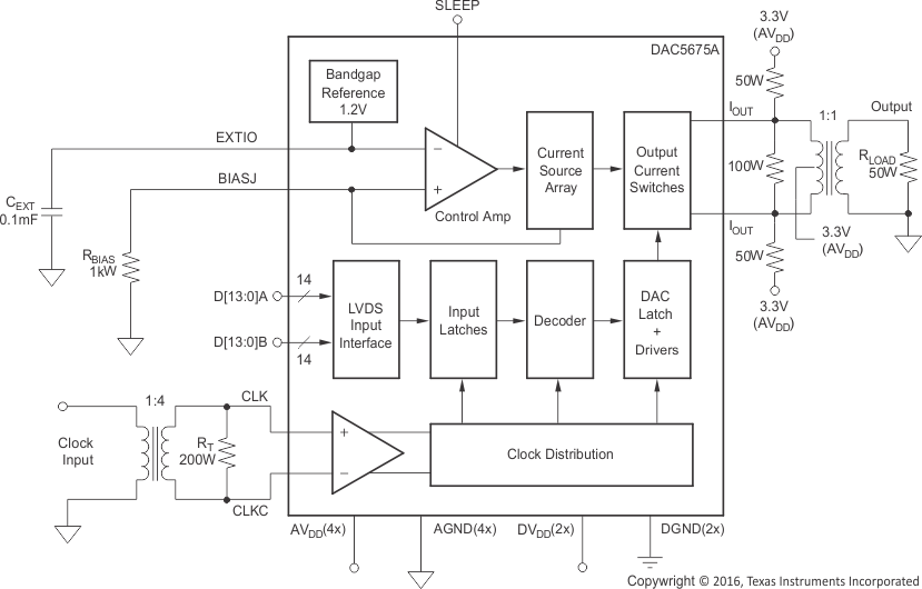
Figure 25 shows a simplified block diagram of the current steering DAC5675A. The DAC5675A consists of a segmented array of NPN-transistor current sinks, capable of delivering a full-scale output current up to 20 mA. Differential current switches direct the current of each current sink to either one of the complementary output nodes IOUT1 or IOUT2. The complementary current output enables differential operation, canceling out common-mode noise sources (digital feed-through, on-chip and PCB noise), dc offsets, and even-order distortion components, and doubling signal output power.
The full-scale output current is set using an external resistor (RBIAS) in combination with an on-chip bandgap voltage reference source (1.2 V) and control amplifier. The current (IBIAS) through resistor RBIAS is mirrored internally to provide a full-scale output current equal to 16 times IBIAS. The full-scale current is adjustable from 20 mA down to 2 mA by using the appropriate bias resistor value.
9.2 Typical Application
A typical application for the DAC5675a is as dual or single carrier transmitter. The DAC is provided with some input digital baseband signal and it outputs an analog carrier.
 Figure 25. Application Schematic
9.2.1 Design Requirements
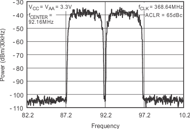
The requirements for this design were to generate a 2-carrier WCDMA signal at an intermediate frequency of 92.16 MHz. The ACPR needs to be better than 65 dBc. For this design example use the parameters shown in Table 1.
Table 1. Design Parameters
| PARAMETER | VALUE |
|---|---|
| Clock rate | 368.64 MHz |
| Input data | 2C WCDMA with IF frequency at 92.16MHz |
| VCC / VAA | 3.3 V |
9.2.2 Detailed Design Procedure
The 2-carrier signal with an intermediate frequency of 92.16 MHz must be created in the digital processor at a sample rate of 368.64 Msps for DAC. These 14 bit samples are placed on the 14b LVDS input port of the DAC.
A differential DAC clock must be generated from a clock source at 368.64 MHz. This must be provided to the CLKIN pins of the DAC.
The IOUOTA and IOUTB differential connections must be connected to a transformer to provide a single ended output. A typical 1:1 impedance transformer is used on the device EVM. The DAC5675AEVM (SLAU080) provides a good reference for this design example.
9.2.3 Application Curves
This spectrum analyzer plot shows the ACPR for the transformer output 2-carrier signal with intermediate frequency of 92.16 MHz. The results meet the system requirements for a minimum of 65 dBc ACPR.
 Figure 26. W-CDMA TM1 Dual Carrier Power vs Frequency