SLVSDP7A February 2017 – May 2017 DLPA1000
PRODUCTION DATA.
- 1 Features
- 2 Applications
- 3 Description
- 4 Revision History
- 5 Pin Configuration and Functions
- 6 Specifications
-
7 Detailed Description
- 7.1 Overview
- 7.2 Functional Block Diagram
- 7.3 Feature Description
- 7.4 Device Functional Modes
- 7.5 Programming
- 7.6
Register Maps
- 7.6.1 Chip ID (CHIPID) Register (address = 0x00h) [reset = A6h]
- 7.6.2 Enable (ENABLE) Register (address = 0x01h) [reset = 3h]
- 7.6.3 Switch Transient Current Limit (IREG) Register (address = 0x02h) [reset = 28h]
- 7.6.4 SW4 LED DC Regulation Current, MSB (SW4MSB) Register (address = 0x03h) [reset = 0h]
- 7.6.5 SW4 LED DC Regulation Current, LSB (SW4LSB) Register (address = 0x04h) [reset = 0h]
- 7.6.6 SW5 LED DC Regulation Current, MSB (SW5MSB) Register (address = 0x05h) [reset = 0h]
- 7.6.7 SW5 LED DC Regulation Current, LSB (SW5LSB) Register (address = 0x06h) [reset = 0h]
- 7.6.8 SW6 LED DC Regulation Current, MSB (SW6MSB) Register (address = 0x07h) [reset = 0h]
- 7.6.9 SW6 LED DC Regulation Current, LSB (SW6LSB) Register (address = 0x08h) [reset = 0h]
- 7.6.10 Analog Front End Control (AFE) Register (address = 0x0Ah) [reset = 0h]
- 7.6.11 Strobe Decode - Break Before Make Timing Control (BBM) Register (address = 0x0Bh) [reset = 0h]
- 7.6.12 Interrupt (INT) Register (address = 0x0Ch) [reset = X]
- 7.6.13 Interrupt Mask (MASK) Register (address = 0x0Dh) [reset = 0h]
- 7.6.14 Password (PASSWORD) Register (address = 0x10h) [reset = 0h]
- 7.6.15 System Configuration (SYSTEM) Register (address = 0x11h) [reset = 0h]
- 7.6.16 EEPROM User Register, Byte0 (BYTE0) (address = 0x20h) [reset = 0h]
- 7.6.17 EEPROM User Register, Byte1 (BYTE1) (address = 0x21h) [reset = 0h]
- 7.6.18 EEPROM User Register, Byte2 (BYTE2) (address = 0x22h) [reset = 0h]
- 7.6.19 EEPROM User Register, Byte3 (BYTE3) (address = 0x23h) [reset = 0h]
- 7.6.20 EEPROM User Register, Byte4 (BYTE4) (address = 0x24h) [reset = 0h]
- 7.6.21 EEPROM User Register, Byte5 (BYTE5) (address = 0x25h) [reset = 0h]
- 7.6.22 EEPROM User Register, Byte6 (BYTE6) (address = 0x26h) [reset = 0h]
- 7.6.23 EEPROM User Register, Byte7 (BYTE7) (address = 0x27h) [reset = 0h]
- 8 Application and Implementation
- 9 Power Supply Recommendations
- 10Layout
- 11Device and Documentation Support
- 12Mechanical, Packaging, and Orderable Information
Package Options
Refer to the PDF data sheet for device specific package drawings
Mechanical Data (Package|Pins)
- YFF|49
Thermal pad, mechanical data (Package|Pins)
Orderable Information
8 Application and Implementation
NOTE
Information in the following applications sections is not part of the TI component specification, and TI does not warrant its accuracy or completeness. TI’s customers are responsible for determining suitability of components for their purposes. Customers should validate and test their design implementation to confirm system functionality.
8.1 Application Information
A DLPC2607 controller can be used with a DLP2000 DMD to provide a compact, reliable, high-efficiency display solution for many different video display applications. DMDs are spatial light modulators which reflect incoming light from an illumination source to one of two directions with the primary direction being into collection optics within a projection lens. The projection lens sends the light to the destination needed for the application. Each application is derived primarily from the optical architecture of the system and the format of the pixel data being input into the DLPC2607.
In display applications using the DLP2000 DMD, the DLPA1000 provides necessary analog functions including analog power supplies and an RGB LED driver to provide a robust and efficient display solution. Display applications of interest include pico-projectors embedded in display devices like smart phones, tablets, cameras, and camcorders. Other applications include wearable (near-eye) displays, battery-powered mobile accessory, interactive display, low latency gaming displays, and digital signage.
8.2 Typical Application
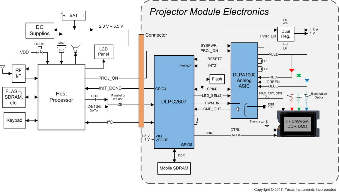
A common application when using DLPA1000 with DLP2000 DMD and DLPC2607 controller is creating a pico-projector embedded in a handheld product. For example, a pico-projector may be embedded in a smart phone, a tablet, a camera, or camcorder. The DLPC2607 in the pico-projector embedded module typically receives images from a host processor within the product as shown in Figure 35. DLPA1000 provides power supply sequencing and controls the LED currents as required by the application.
 Figure 35. Typical Standalone Projector System Block Diagram
8.2.1 Design Requirements
A pico-projector is created by using a DLP chipset comprised of a DMD such as the DLP2000, a controller such as the DLPC2607, and a PMIC/LED driver such as the DLPA1000. The DLPA1000 provides the needed analog functions for the projector, the DLPC2607 does the digital image processing, and the DMD is the display device for producing the projected image. In addition to the three critical DLP components, other chips may be needed for the full system design, such as the battery (SYSPWR), a regulated 1.8-V supply for the controller VIO, and a regulated 1-V supply for the controller VCORE.
The DLPA1000 provides power to the illumination source for the DMD, typically from red, green, and blue LEDs. These are often contained in three separate packages, but sometimes more than one color of LED die may be in the same package to reduce the overall size of the pico-projector. The entire pico-projector can be turned on and off by using a single signal called PROJ_ON. When PROJ_ON is high, the projector turns on and begins displaying images. When PROJ_ON is set low, the projector turns off and draws just microamps of current on SYSPWR. When PROJ_ON is set low, the 1.8-V and 1-V supplies can remain active to be used by other non-projector sections of the product.
8.2.2 Detailed Design Procedure
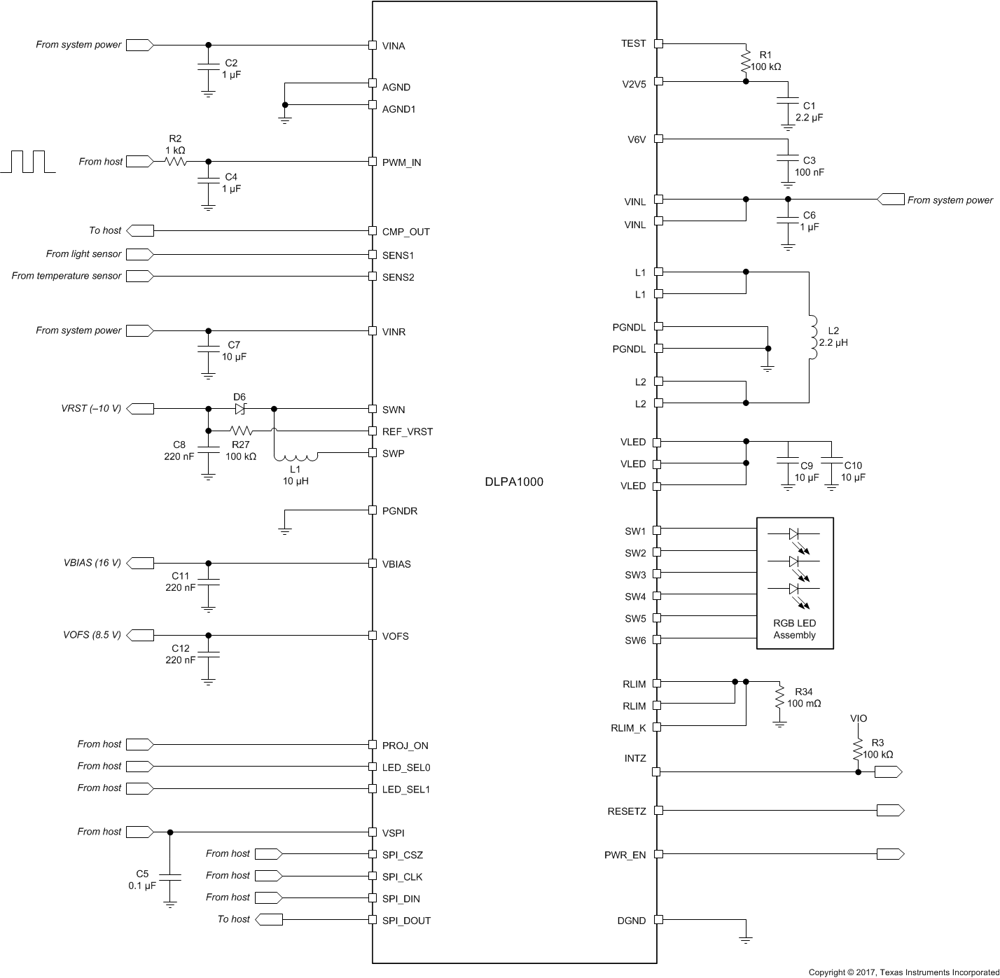
The DLPA1000 contains a buck-boost regulator for the LEDs, boost regulators for the DMD rails, and internal LDOs for logic state control and operation. Each regulator requires a few external components to operate, referenced by their designators in Figure 36 and Figure 38, and all capacitors should maintain the recommended values at expected operating temperatures and bias voltages.
 Figure 36. Schematic
8.2.2.1 VLED Buck-Boost
The VLED buck-boost provides the necessary voltages for the LED array capable of supporting both common anode and cathode-cathode-anode RGB LEDs. Configurations for both packages are detailed in the RGB Strobe Decoder section. Alternatively, a design could utilize an optical engine from an OEM that specializes in designing optics for DLP projectors, which typically integrate the LEDs and DMD into a single module. Current sensing through the LEDs is accomplished with a high-precision (0.1%) 100-mΩ sense resistor (R34) connecting RLIM to GND, with a separate trace providing a Kelvin connection to RLIM_K directly from the pad of the sense resistor.
The VLED buck-boost utilizes a single 2.2-µH inductor (L2) to generate the voltages for the LED array, bridging the pins labeled L1 to the pins labeled L2. The buck-boost also requires a 1-µF input bypass capacitor (C6) connecting VINL to GND, and two 10-µF output filter capacitors (C9 and C10) connecting VLED to GND. Ensure the inductor can handle the expected operating currents and refer to Calculating Inductor Peak Current to calculate the expected peak current for a design that can saturate the inductor's core.
8.2.2.1.1 Calculating Inductor Peak Current
To properly configure the DLPA1000 device, a 2.2-µH inductor (L2) must be connected between pins L1 and L2. The peak current for the inductor in steady state operation can be calculated.
Equation 1 shows how to calculate the peak current I1 in step down mode operation and Equation 2 shows how to calculate the peak current I2 in boost mode operation. VIN1 is the maximum input voltage VIN2 is the minimum input voltage, f is the switching frequency (2.25 MHz) and L the inductor value (2.2 µH).


The critical current value for selecting the right inductor is the higher value of I1 and I2. It also needs to be taken into account that load transients and error conditions may cause higher inductor currents. This also needs to be taken into account when selecting an appropriate inductor. Internally the switching current is limited to 2.2 A.
8.2.2.2 DMD Supplies
The PMIC also utilizes a single inductor (L1) to generate the low-current –10-V, 16-V, and 8.5-V supplies. Connect the inductor from SWP to SWN, and use a Schottky diode (D6) to generate the –10 V by connecting the cathode of the diode to the SWN side of the inductor and the anode of the diode to the load (VRST). Place a 220-nF filter cap (C8) from VRST to GND and bridge VRST to the feedback pin (REF_VRST) using a 100-kΩ resistor (R27). Bypass VINR to GND using a 10-µF capacitor (C7), and ensure VBIAS and VOFS each have dedicated 220-nF output filter capacitors (C11 and C12).
8.2.2.3 LDOs and Digital Logic
Ensure V2V5 has a 2.2-µF output capacitor (C1), and that V6V has a 100-nF output capacitor (C3). It is critical that V2V5 externally connects to the TEST pin (R1), otherwise the PMIC will be unable to operate. UVLO for this device is typically 2.3 V.
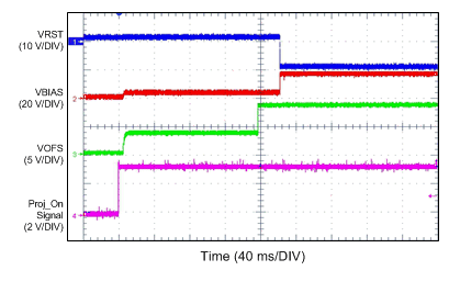
8.2.3 Application Curve
