SLVSDP7A February 2017 – May 2017 DLPA1000
PRODUCTION DATA.
- 1 Features
- 2 Applications
- 3 Description
- 4 Revision History
- 5 Pin Configuration and Functions
- 6 Specifications
-
7 Detailed Description
- 7.1 Overview
- 7.2 Functional Block Diagram
- 7.3 Feature Description
- 7.4 Device Functional Modes
- 7.5 Programming
- 7.6
Register Maps
- 7.6.1 Chip ID (CHIPID) Register (address = 0x00h) [reset = A6h]
- 7.6.2 Enable (ENABLE) Register (address = 0x01h) [reset = 3h]
- 7.6.3 Switch Transient Current Limit (IREG) Register (address = 0x02h) [reset = 28h]
- 7.6.4 SW4 LED DC Regulation Current, MSB (SW4MSB) Register (address = 0x03h) [reset = 0h]
- 7.6.5 SW4 LED DC Regulation Current, LSB (SW4LSB) Register (address = 0x04h) [reset = 0h]
- 7.6.6 SW5 LED DC Regulation Current, MSB (SW5MSB) Register (address = 0x05h) [reset = 0h]
- 7.6.7 SW5 LED DC Regulation Current, LSB (SW5LSB) Register (address = 0x06h) [reset = 0h]
- 7.6.8 SW6 LED DC Regulation Current, MSB (SW6MSB) Register (address = 0x07h) [reset = 0h]
- 7.6.9 SW6 LED DC Regulation Current, LSB (SW6LSB) Register (address = 0x08h) [reset = 0h]
- 7.6.10 Analog Front End Control (AFE) Register (address = 0x0Ah) [reset = 0h]
- 7.6.11 Strobe Decode - Break Before Make Timing Control (BBM) Register (address = 0x0Bh) [reset = 0h]
- 7.6.12 Interrupt (INT) Register (address = 0x0Ch) [reset = X]
- 7.6.13 Interrupt Mask (MASK) Register (address = 0x0Dh) [reset = 0h]
- 7.6.14 Password (PASSWORD) Register (address = 0x10h) [reset = 0h]
- 7.6.15 System Configuration (SYSTEM) Register (address = 0x11h) [reset = 0h]
- 7.6.16 EEPROM User Register, Byte0 (BYTE0) (address = 0x20h) [reset = 0h]
- 7.6.17 EEPROM User Register, Byte1 (BYTE1) (address = 0x21h) [reset = 0h]
- 7.6.18 EEPROM User Register, Byte2 (BYTE2) (address = 0x22h) [reset = 0h]
- 7.6.19 EEPROM User Register, Byte3 (BYTE3) (address = 0x23h) [reset = 0h]
- 7.6.20 EEPROM User Register, Byte4 (BYTE4) (address = 0x24h) [reset = 0h]
- 7.6.21 EEPROM User Register, Byte5 (BYTE5) (address = 0x25h) [reset = 0h]
- 7.6.22 EEPROM User Register, Byte6 (BYTE6) (address = 0x26h) [reset = 0h]
- 7.6.23 EEPROM User Register, Byte7 (BYTE7) (address = 0x27h) [reset = 0h]
- 8 Application and Implementation
- 9 Power Supply Recommendations
- 10Layout
- 11Device and Documentation Support
- 12Mechanical, Packaging, and Orderable Information
Package Options
Refer to the PDF data sheet for device specific package drawings
Mechanical Data (Package|Pins)
- YFF|49
Thermal pad, mechanical data (Package|Pins)
Orderable Information
7 Detailed Description
7.1 Overview
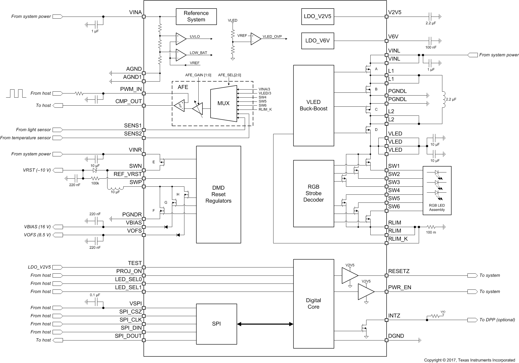
DLPA1000 is a power management IC optimized for TI DLP® Pico™ Projector systems and meant for use in either embedded or accessory mobile phone applications. For embedded applications, the projector is built into the mobile phone and operates from the mobile phone’s single cell battery. In accessory applications, the projector resides in its own enclosure and has its own battery or external power supply and operates as a stand-alone device.
DLPA1000 contains a complete LED driver and can supply up to 1 A per LED. Integrated high-current switches are included for sequentially selecting a red, green, or blue LED. The DLPA1000 also contains three regulated DC supplies for the DMD: VBIAS, VRST and VOFS.
The DLPA1000 contains a serial periphery interface (SPI) used for setting the configuration. Using SPI, currents can be set independently for each LED with 10-bit resolution. Other features included are the generation of the system reset, power sequencing, input signals for sequentially selecting the active LED, IC self-protection, and an analog multiplexer and comparator to support A/D conversion of system parameters.
7.2 Functional Block Diagram
7.3 Feature Description
7.3.1 DMD Regulators
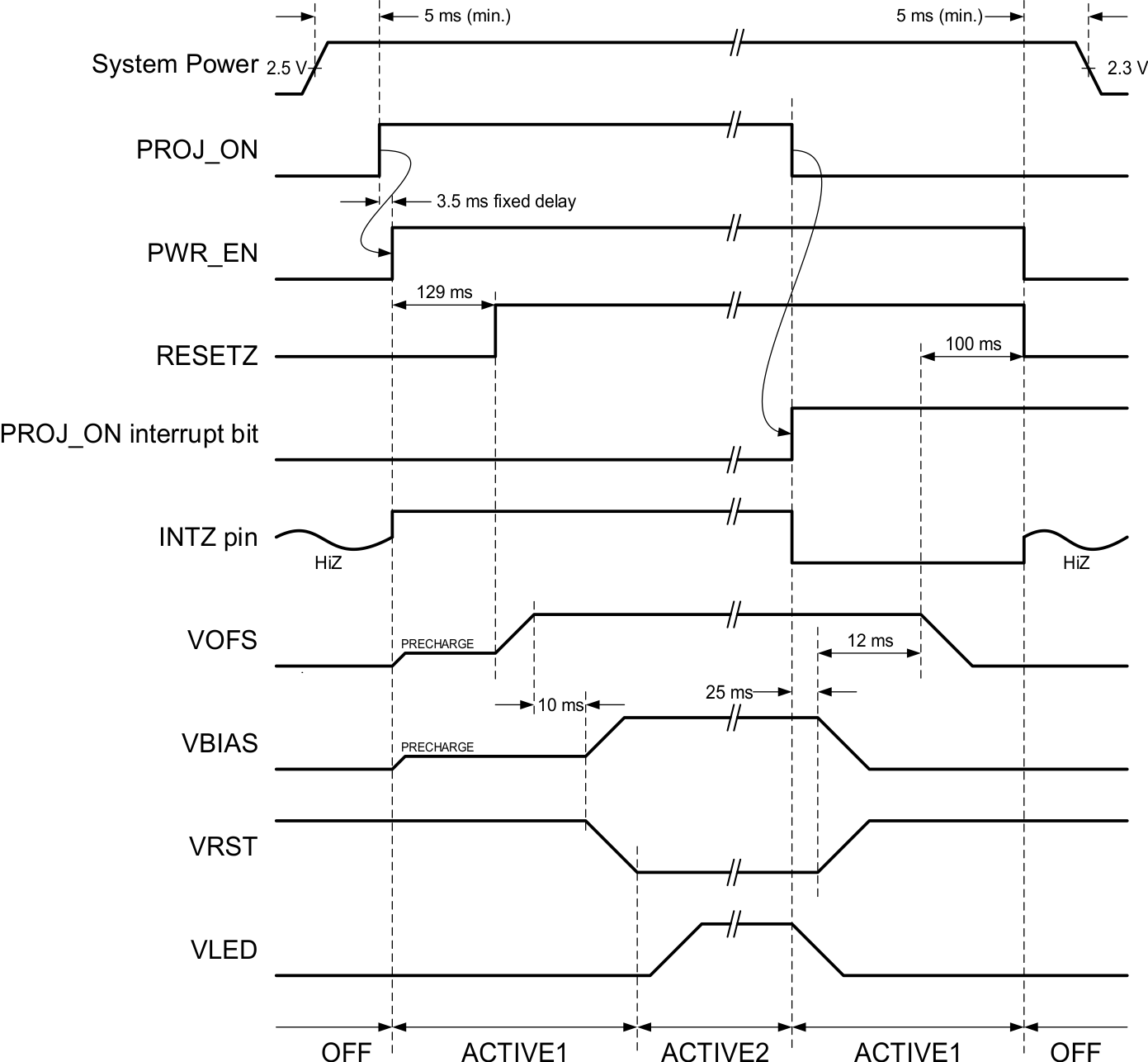
DLPA1000 contains three switch-mode power supplies that power the DMD. These rails are VOFS, VBIAS, and VRST. 100 ms after pulling the PROJ_ON pin high, VOFS is powered up, followed by VBIAS and VRST with an additional 10-ms delay. Only after all three rails are enabled can the LED driver and STROBE DECODER circuit be enabled. If any one of the rails encounters a fault such as an output short, all three rails are disabled simultaneously. The detailed power-up and power-down diagram is shown in Figure 3.
7.3.2 RGB Strobe Decoder
DLPA1000 contains RGB color-sequential circuitry that is composed of six NMOS switches, the LED driver, the strobe decoder and the LED current control. The NMOS switches are connected to the terminals of the external LED package and turn the currents through the LEDs on and off. The strobe decoder controls the gates of the NMOS switches according to the LED_SEL[1:0] input signals and the MAP bit of the SYSTEM register. The MAP bit selects one of two package configurations. A ‘1’ indicates a cathode-cathode-anode package and a ‘0’ indicates the common anode package. The two package connections are shown in Figure 4 and the corresponding switch map in Table 1 and Table 2.
The LED_SEL[1:0] signals typically receive a rotating code switching from RED to GREEN to BLUE and then back to RED. When the LED_SEL[1:0] input signals select a specific color, the NMOSFETs are controlled based on the color selected, and a 10-bit current control DAC for this color is selected that provides a color correction current to the RGB LEDs feedback control network.
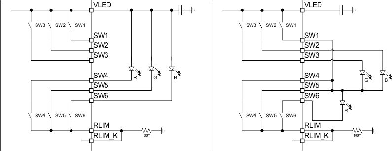 Figure 4. LEFT: Switch Connection for a Common-Anode LED Assembly
RIGHT: Switch Connection for a Cathode-Cathode-Anode LED Assembly
Table 1. Switch Positions for Common Anode RGB LEDs (MAP = 0)
| MAP = 0 (Common Anode, Default) | |||||||
|---|---|---|---|---|---|---|---|
| LED_SEL[1:0] | SW6 | SW5 | SW4 | SW3 | SW2 | SW1 | IDAC input |
| 0x00h | open | open | open | closed | closed | closed | N/A |
| 0x01h | open | open | closed | closed | closed | closed | SW4_IDAC[9:0] |
| 0x02h | open | closed | open | closed | closed | closed | SW5_IDAC[9:0] |
| 0x03h | closed | open | open | closed | closed | closed | SW6_IDAC[9:0] |
Table 2. Switch Positions for Cathode-Cathode-Anode RGB LEDs (MAP = 1)
| MAP = 1 (Cathode-Cathode-Anode LED Arrangement) | |||||||
|---|---|---|---|---|---|---|---|
| LED_SEL[1:0] | SW6 | SW5 | SW4 | SW3 | SW2 | SW1 | IDAC input |
| 0x00h | open | open | open | open | open | open | N/A |
| 0x01h | closed | open | open | open | open | closed | SW4_IDAC[9:0] |
| 0x02h | open | closed | closed | closed | open | open | SW5_IDAC[9:0] |
| 0x03h | open | closed | closed | open | closed | open | SW6_IDAC[9:0] |
The switching of the six NMOS switches is controlled such that switches are returned to the OPEN position first before the CLOSED connections are made (Break Before Make). The dead time between opening and closing switches is controlled through the BBM register. Switches that already are in the CLOSED position and are to remain in the CLOSED state according to the SWCNTRL register, are not opened during the BBM delay time.
7.3.3 LED Current Control
DLPA1000 provides time-sequential circuitry to drive three LEDs with independent current control. A system based on a common anode LED configuration is shown in Figure 6 and consists of a buck-boost converter which provides the voltage to drive the LEDs, three switches connected to the cathodes of the LEDs, a 100-mΩ resistor used to sense the LED current, and a current DAC to control the LED current.
The STROBE DECODER controls the switch positions as described in the section above. With all switches in the OPEN position, the buck-boost output assumes an output voltage of 3.5 V.
For a common-anode RGB LED configuration (MAP = 0, default), the BUCK-BOOST output voltage (VLED) assumes a value such that the voltage drop across the sense resistor equals (SW4_IDAC[9:0] × 100 mΩ) when SW4 is closed. The exact value of VLED depends on the current setting and the voltage drop across the LED but is limited to 6.5 V. When the STROBE decoder switches from SW4 to SW5, the Buck-Boost assumes a new output voltage such that the sense voltage equals (SW5_IDAC[9:0] × 100 mΩ), and finally, when SW6 is selected, V(RLIM_K) is regulated to (SW6_IDAC[9:0] × 100 mΩ).
Similarly, the regulation current setting switches from SW4_IDAC[9:0] to SW5_IDAC[9:0] to SW6_IDAC[9:0] depending on the LED_SEL[1:0] setting with a MAP setting of 1 (cathode-cathode-anode configuration). See Table 2 for details.
7.3.3.1 LED Current Accuracy
LED drive current is controlled by a current DAC (digital to analog converter) and can be set independently for switch SW4, SW5, and SW6. The DAC is trimmed to achieve a LED drive current of 272 mA at code 0x100h with an accuracy of ±14 mA. The first order gain-error of the DAC can be neglected, therefore the LED driver current accuracy of ±14 mA can be assumed over the full current range. For example, at full-scale (SWx_IDAC[9:0] = 0x3FFh) the LED current is regulated to 1030 mA ±14 mA or ±1.4%. At the lowest setting (0x001h) the LED current is regulated to 20 mA ±14 mA and the resulting relative error is large; however this is not a typical operating point for a projector application. A typical drive current for projection LEDs is 300 mA and the resulting regulation error is < 5%.
7.3.3.2 Transient Current Limiting
Typically the forward voltages of the GREEN and BLUE diodes are close to each other (~3 V to 4 V) but Vf of the RED diode is significantly lower (1.8 V to 2.5 V). This can lead to a current spike in the RED diode when the strobe controller switches from GREEN or BLUE to RED because VLED is regulated to a higher voltage than required to drive the RED diode. DLPA1000 provides transient current limiting for each switch to limit the current in the LEDs during the transition. The transient current limit value is controlled through the ILIM[2:0] bits in the IREG register. The same register also contains three bits to select which switch employs the transient current limiting feature. In a typical application it is required only for the RED diode and the ILIM[2:0] value should be set approximately 10% higher than the DC regulation current. The effect that the transient current limit has on the LED current is shown in Figure 5.
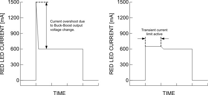
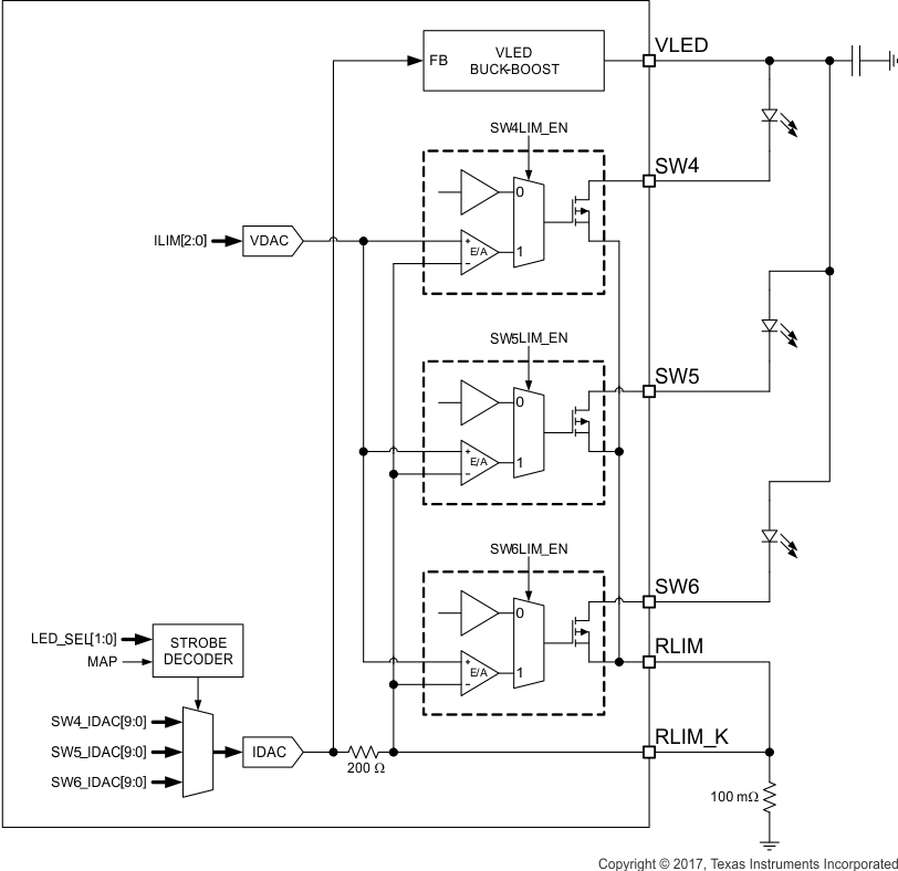 Figure 6. Block Diagram of the LED Driver Circuitry
7.3.4 Measurement System
The measurement system is composed of a 8:1 analog multiplexer (MUX), a programmable-gain amplifier and a comparator. It works together with the DPP processor to provide:
- White-point correction (WPC) by independently adjusting the R/G/B LED currents, after measuring the brightness of each color from an external light sensor.
- A measurement of the battery voltage.
- A measurement of the LED forward voltage.
- A measurement of the exact LED current.
- A measurement of temperature as derived by measuring the voltage across an external thermistor.
A block diagram of the measurement system is shown in Figure 7.
 Figure 7. Block Diagram of the Measurement System
Table 3. Recommended Configuration of the AFE for Different Input Selections
| AFE_SEL[2:0] | SELECTED INPUT | RECOMMENDED GAIN SETTING AFE-GAIN[1:0] |
RECOMMENDED SETTING OF AFE_CAL_DIS BIT |
|---|---|---|---|
| 0x00h | SENS2 | 0x01h (1x) | Setting has no effect on measurement |
| 0x01h | VLED | 0x01h (1x) | Setting has no effect on measurement |
| 0x02h | VINA | 0x01h (1x) | Setting has no effect on measurement |
| 0x03h | SENS1 | 0x01h (1x) | Setting has no effect on measurement |
| 0x04h | RLIM_K | 0x03h (18x) | Set to 1 if sense voltage is > 100 mV, otherwise set to 0 (default). |
| 0x05h | SW4 | 0x02h (9.5x) | Set to 1 if sense voltage is > 200 mV, otherwise set to 0 (default). |
| 0x06h | SW5 | 0x02h (9.5x) | Set to 1 if sense voltage is > 200 mV, otherwise set to 0 (default). |
| 0x07h | SW6 | 0x02h (9.5x) | Set to 1 if sense voltage is > 200 mV, otherwise set to 0 (default). |
7.3.5 Protection Circuits
DLPA1000 has several protection circuits to protect the IC as well as the system from damage due to excessive power consumption, die temperature, or over-voltages. These circuits are described below.
7.3.5.1 Thermal Warning (HOT) and Thermal Shutdown (TSD)
DLPA1000 continuously monitors the junction temperature and issues a HOT interrupt if temperature exceeds the HOT threshold. If the temperature continues to increase above the thermal shutdown threshold, all rails are disabled and the TSD bit in the INT register is set. Once the temperature drops by 15°C, the output rails are powered up in sequence and normal operation resumes (DMD_EN bit is not reset by TSD fault).
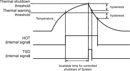 Figure 8. Definition of the Thermal Shutdown and Hot-Die Temperature Warning
7.3.5.2 Low Battery Warning (BAT_LOW) and Undervoltage Lockout (UVLO)
If the battery voltage drops below the BAT_LOW threshold (typically 3 V) the BAT_LOW interrupt is issued but normal operation continues. Once the battery drops below the undervoltage threshold (typically 2.3 V) the UVLO interrupt is issued, all rails are powered down in sequence, the DMD_EN bit is reset, and the part enters STANDBY mode. The power rails cannot be re-enabled before the input voltage recovers to > 2.4 V. To re-enable the rails, the PROJ_ON pin must be toggled.
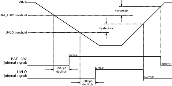 Figure 9. Undervoltage Lockout is Asserted When the Input Supply Drops Below the UVLO Threshold
7.3.5.3 DMD Regulator Fault (DMD_FLT)
The DMD regulator is continuously monitored to check if the output rails are in regulation and if the inductor current increases as expected during a switching cycle. If either one of the output rails drops out of regulation (e.g. due to a shorted output) or the inductor current does not increase as expected during a switching cycle (due to a disconnected inductor), the DMD_FLT interrupt bit is set in the INT register, the DMD_EN bit is reset, and the DMD regulator is shut down. Resetting the DMD_EN bit also causes the LED driver to power down. To restart the system, the PROJ_ON pin must be toggled.
7.3.5.4 V6V Power-Good (V6V_PGF) Fault
The VLED buck-boost requires the V6V rail for proper operation. The rail is continuously monitored and should the output drop below the power-good threshold, the V6V_PGF bit is set. The buck-boost is disabled and attempts to restart automatically.
7.3.5.5 VLED Over-Voltage (VLED_OVP) Fault
If the buck-boost output voltage rises above 6.5 V, the VLED_OVP interrupt is set but the buck-boost regulator is not turned off. A typical condition to cause this fault is an open LED.
7.3.6 Interrupt Pin (INTZ)
The interrupt pin is used to signal events and fault conditions to the host processor. Whenever a fault or event occurs in the IC, the corresponding interrupt bit is set in the INT register, and the open-drain output is pulled low. The INTZ pin is released (returns to HiZ state) and fault bits are cleared when the INT register is read by the host. However, if a failure persists, the corresponding INT bit remains set and the INTZ pin is pulled low again after a maximum of 32 µs.
Interrupt events include fault conditions such as power-good faults, over-voltage, over-temperature shut-down, and under-voltage lock-out.
The MASK register is used to mask events from generating interrupts, i.e. from pulling the INTZ pin low. The MASK settings affect the INTZ pin only and have no impact on protection and monitor circuits themselves. When an interrupt is masked, the event causing the interrupt still sets the corresponding bit in the INT register. However, it does not pull the INTZ pin low.
Note that persisting fault conditions such as thermal shutdown can cause the INTZ pin to be pulled low for an extended period of time which can keep the host in a loop trying to resolve the interrupt. If this behavior is not desired, set the corresponding mask bit after receiving the interrupt and keep polling the INT register to see when the fault condition has disappeared. After the fault is resolved, unmask the interrupt bit again.
7.3.7 Serial Peripheral Interface (SPI)
DLPA1000 provides a 4-wire SPI port that supports high-speed serial data transfers up to 33.3 MHz. Register and data buffer write and read operations are supported. The SPI_CSZ input serves as the active low chip select for the SPI port. The SPI_CSZ input must be forced low in order to write or read registers and data buffers. When SPI_CSZ is forced high, the data at the SPI_DIN input is ignored, and the SPI_DOUT output is forced to a high-impedance state. The SPI_DIN input serves as the serial data input for the port; the SPI_DOUT output serves as the serial data output. The SPI_CLK input serves as the serial data clock for both the input and output data. Data is latched at the SPI_DIN input on the rising edge of SPI_CLK, while data is clocked out of the SPI_DOUT output on the falling edge of SPI_CLK. Figure 10 illustrates the SPI port protocol. Byte 0 is referred to as the command byte, where the most significant bit is the write/not read bit. For the W/nR bit, a 1 indicates a write operation, while a 0 indicates a read operation. The remaining seven bits of the command byte are the register address targeted by the write or read operation. The SPI port supports write and read operations for multiple sequential register addresses through the implementation of an auto-increment mode. As shown in Figure 10, the auto-increment mode is invoked by simply holding the SPI_CSZ input low for multiple data bytes. The register address is automatically incremented after each data byte transferred, starting with the address specified by the command byte. After reaching address 0x7Fh the address pointer jumps back to 0x00h.
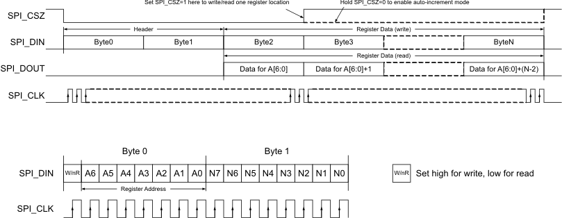 Figure 10. SPI Protocol
7.4 Device Functional Modes
Table 4. Modes of Operation
| MODE | DESCRIPTION |
|---|---|
| OFF | This is the lowest-power mode of operation. All power functions are turned off, registers are reset to their default values and the IC does not respond to SPI commands. RESETZ and PWR_EN pins are pulled low. The IC will enter OFF mode whenever the PROJ_ON pin is pulled low. |
| RESET | Logic core and registers are reset to default values, the IC does not respond to SPI commands, RESETZ and PWR_EN pins are pulled low, but the analog reference system is kept alive. The device enters RESET state when the input voltage drops below the UVLO threshold. |
| STANDBY | All power functions are turned off but the IC does respond to the SPI interface. The device enters STANDBY mode when PROJ_ON pins is high, but DMD_EN bit is set to 0. Also, device enters STANDBY mode when a fault on the DMD regulator occurs or the temperature increases above thermal shutdown threshold (TSD).(1) |
| ACTIVE1 | The DMD supplies are powered up but LED power (VLED) and the STROBE DECODER are disabled. PROJ_ON pin must be high, DMD_EN bit must be set to 1, and VLED_EN bit set to 0. |
| ACTIVE2 | DMD supplies, LED power and STROBE DECODER are enabled. PROJ_ON pin must be high and DMD_EN and VLED_EN bits must both be set to 1. |
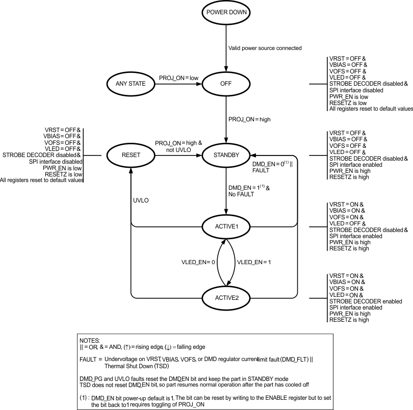 Figure 11. State Diagram
7.5 Programming
7.5.1 Password Protected Registers
Register address 0x11h through 0x27h can be read-accessed the same way as any other register but are protected against accidental write operations through the PASSWORD register (address 0x10h). To write to a protected register, first:
- Write data 0xBAh to register address 0x10h, then
- Write data 0xBEh to register address 0x10h.
Both writes must be consecutive, i.e. there must be no other read or write operation in between sending the two bytes. Once the password has been successfully written, register 0x11h through 0x27h are unlocked and can be write accessed using the regular SPI protocol. They remain unlocked until any byte other than 0xBAh is written to the PASSWORD register or the part is power cycled.
To check if the registers are unlocked, read back the PASSWORD register. If the data returned is 0x00h, the registers are locked. If the PASSWORD register returns 0x01h, the registers are unlocked.
7.6 Register Maps
Table 5. Register Address Map
| Address | Acronym | Register Name | Section |
|---|---|---|---|
| 0x00h | CHIPID | Chip revision register | Go |
| 0x01h | ENABLE | Enable register | Go |
| 0x02h | IREG | Transient-current limit settings | Go |
| 0x03h | SW4MSB | Regulation current MSBs, SW4 | Go |
| 0x04h | SW4LSB | Regulation current LSBs, SW4 | Go |
| 0x05h | SW5MSB | Regulation current MSBs, SW5 | Go |
| 0x06h | SW5LSB | Regulation current LSBs, SW5 | Go |
| 0x07h | SW6MSB | Regulation current MSBs, SW6 | Go |
| 0x08h | SW6LSB | Regulation current LSBs, SW6 | Go |
| 0x09h | RESERVED | Reserved | |
| 0x0Ah | AFE | AFE (MUX) control | Go |
| 0x0Bh | BBM | Break before make timing | Go |
| 0x0Ch | INT | Interrupt register | Go |
| 0x0Dh | INT MASK | Interrupt mask register | Go |
| 0x10h | PASSWORD | Password register | Go |
| 0x11h | SYSTEM | System configuration register | Go |
| 0x20h | BYTE0 | User EEPROM, Byte0 | Go |
| 0x21h | BYTE1 | User EEPROM, Byte1 | Go |
| 0x22h | BYTE2 | User EEPROM, Byte2 | Go |
| 0x23h | BYTE3 | User EEPROM, Byte3 | Go |
| 0x24h | BYTE4 | User EEPROM, Byte4 | Go |
| 0x25h | BYTE5 | User EEPROM, Byte5 | Go |
| 0x26h | BYTE6 | User EEPROM, Byte6 | Go |
| 0x27h | BYTE7 | User EEPROM, Byte7 | Go |
7.6.1 Chip ID (CHIPID) Register (address = 0x00h) [reset = A6h]
| 7 | 6 | 5 | 4 | 3 | 2 | 1 | 0 |
| CHIPID[7:0] | |||||||
| R-A6h | |||||||
| LEGEND: R/W = Read/Write; R = Read only; -n = value after reset |
Table 6. CHIPID Register Field Descriptions
| Bit | Field | Type | Reset | Description |
|---|---|---|---|---|
| 7-0 | CHIPID | R | A6h | 1010 0000b = DLPA1000 (Rev 1p0) 1010 0010b = DLPA1000 (Rev 1p1) 1010 0110b = DLPA1000 (Rev 1p2) |
7.6.2 Enable (ENABLE) Register (address = 0x01h) [reset = 3h]
| 7 | 6 | 5 | 4 | 3 | 2 | 1 | 0 |
| RESERVED | DMD_EN | VLED_EN | |||||
| R-0h | R/W-1h | R/W-1h | |||||
| LEGEND: R/W = Read/Write; R = Read only; -n = value after reset |
Table 7. ENABLE Register Field Descriptions
| Bit | Field | Type | Reset | Description |
|---|---|---|---|---|
| 7-2 | RESERVED | R | 0h | N/A |
| 1 | DMD_EN | R/W | 1h | DMD Regulator enable/status bit 0b = disabled (OFF) 1b = enabled (ON) NOTE: Power-up default is 1. Once set to 0, the PROJ_ON pin must be toggled to set the bit back to 1. If bit is set to 0, VLED buck-boost will automatically be disabled. |
| 0 | VLED_EN | R/W | 1h | VLED Buck-Boost enable bit 0b = disabled (OFF) 1b = enabled (ON) NOTE: Bit does not reflect current status of VLED buck-boost. NOTE: If VLED is disabled, RGB Strobe Decoder will automatically be disabled |
7.6.3 Switch Transient Current Limit (IREG) Register (address = 0x02h) [reset = 28h]
| 7 | 6 | 5 | 4 | 3 | 2 | 1 | 0 |
| RESERVED | ILIM[2:0] | SW6LIM_EN | SW5LIM_EN | SW4LIM_EN | |||
| R-0h | R/W-5h | R/W-0h | R/W-0h | R/W-0h | |||
| LEGEND: R/W = Read/Write; R = Read only; -n = value after reset |
Table 8. IREG Register Field Descriptions
| Bit | Field | Type | Reset | Description |
|---|---|---|---|---|
| 7-6 | RESERVED | R | 0h | N/A |
| 5-3 | ILIM[2:0] | R/W | 5h | Transient current-limit 000b = 260 mA 001b = 300 mA 010b = 345 mA 011b = 385 mA 100b = 440 mA 101b = 660 mA 110b = 880 mA 111b = 1250 mA NOTE: Transient current limit should always be set higher than regulation current |
| 2 | SW6LIM_EN | R/W | 0h | Transient current-limit enable for SW6 0b = transient current-limit is disabled 1b = transient current-limit is enabled |
| 1 | SW5LIM_EN | R/W | 0h | Transient current-limit enable for SW5 0b = transient current-limit is disabled 1b = transient current-limit is enabled |
| 0 | SW4LIM_EN | R/W | 0h | Transient current-limit enable for SW4 0b = transient current-limit is disabled 1b = transient current-limit is enabled |
7.6.4 SW4 LED DC Regulation Current, MSB (SW4MSB) Register (address = 0x03h) [reset = 0h]
| 7 | 6 | 5 | 4 | 3 | 2 | 1 | 0 |
| RESERVED | SW4_IDAC[9:8] | ||||||
| R-0h | R/W-0h | ||||||
| LEGEND: R/W = Read/Write; R = Read only; -n = value after reset |
Table 9. SW4MSB Register Field Descriptions
| Bit | Field | Type | Reset | Description |
|---|---|---|---|---|
| 7-2 | RESERVED | R | 0h | N/A |
| 1-0 | SW4_IDAC[9:8] | R/W | 0h | Switch4 DC regulation, most significant byte (MSB) |
7.6.5 SW4 LED DC Regulation Current, LSB (SW4LSB) Register (address = 0x04h) [reset = 0h]
| 7 | 6 | 5 | 4 | 3 | 2 | 1 | 0 |
| SW4_IDAC[7:0] | |||||||
| R/W-0h | |||||||
| LEGEND: R/W = Read/Write; R = Read only; -n = value after reset |
Table 10. SW4LSB Register Field Descriptions
| Bit | Field | Type | Reset | Description |
|---|---|---|---|---|
| 7-0 | SW4_IDAC[7:0] | R/W | 0h | Switch4 DC current limit, least significant byte (MSB) |
| SW4_IDAC[9:0] | LED CURRENT(1) | SW4_IDAC[9:0] | LED CURRENT(1) | SW4_IDAC[9:0] | LED CURRENT(1) | SW4_IDAC[9:0] | LED CURRENT(1) |
|---|---|---|---|---|---|---|---|
| 0x000h | 0 mA | 0x100h | 272 mA | 0x200h | 525 mA | 0x300h | 777.99 mA |
| 0x001h | 19.99 mA | 0x101h | 272.99 mA | 0x201h | 525.98 mA | 0x301h | 778.98 mA |
| 0x002h | 20.98 mA | 0x102h | 273.98 mA | 0x202h | 526.97 mA | 0x302h | 779.97 mA |
| ... | ... | ... | ... | ... | ... | ... | ... |
| 0x0FEh | 270.02 mA | 0x1FEh | 523.602 mA | 0x2FEh | 776.02 mA | 0x3FEh | 1029.01 mA |
| 0x0FFh | 271.01 mA | 0x1FFh | 524.01 mA | 0x2FFh | 777 mA | 0x3FFh | 1030 mA |
7.6.6 SW5 LED DC Regulation Current, MSB (SW5MSB) Register (address = 0x05h) [reset = 0h]
| 7 | 6 | 5 | 4 | 3 | 2 | 1 | 0 |
| RESERVED | SW5_IDAC[9:8] | ||||||
| R-0h | R/W-0h | ||||||
| LEGEND: R/W = Read/Write; R = Read only; -n = value after reset |
Table 11. SW5MSB Register Field Descriptions
| Bit | Field | Type | Reset | Description |
|---|---|---|---|---|
| 7-2 | RESERVED | R | 0h | N/A |
| 1-0 | SW5_IDAC[9:8] | R/W | 0h | Switch5 DC regulation, most significant byte (MSB) |
7.6.7 SW5 LED DC Regulation Current, LSB (SW5LSB) Register (address = 0x06h) [reset = 0h]
| 7 | 6 | 5 | 4 | 3 | 2 | 1 | 0 |
| SW5_IDAC[7:0] | |||||||
| R/W-0h | |||||||
| LEGEND: R/W = Read/Write; R = Read only; -n = value after reset |
Table 12. SW5LSB Register Field Descriptions
| Bit | Field | Type | Reset | Description |
|---|---|---|---|---|
| 7-0 | SW5_IDAC[7:0] | R/W | 0h | Switch5 DC current limit, least significant byte (LSB) |
| SW5_IDAC[9:0] | LED CURRENT(1) | SW5_IDAC[9:0] | LED CURRENT(1) | SW5_IDAC[9:0] | LED CURRENT(1) | SW5_IDAC[9:0] | LED CURRENT(1) |
|---|---|---|---|---|---|---|---|
| 0x000h | 0 mA | 0x100h | 272 mA | 0x200h | 525 mA | 0x300h | 777.99 mA |
| 0x001h | 19.99 mA | 0x101h | 272.99 mA | 0x201h | 525.98 mA | 0x301h | 778.98 mA |
| 0x002h | 20.98 mA | 0x102h | 273.98 mA | 0x202h | 526.97 mA | 0x302h | 779.97 mA |
| ... | ... | ... | ... | ... | ... | ... | ... |
| 0x0FEh | 270.02 mA | 0x1FEh | 523.602 mA | 0x2FEh | 776.02 mA | 0x3FEh | 1029.01 mA |
| 0x0FFh | 271.01 mA | 0x1FFh | 524.01 mA | 0x2FFh | 777 mA | 0x3FFh | 1030 mA |
7.6.8 SW6 LED DC Regulation Current, MSB (SW6MSB) Register (address = 0x07h) [reset = 0h]
| 7 | 6 | 5 | 4 | 3 | 2 | 1 | 0 |
| RESERVED | SW6_IDAC[9:8] | ||||||
| R-0h | R/W-0h | ||||||
| LEGEND: R/W = Read/Write; R = Read only; -n = value after reset |
Table 13. SW6MSB Register Field Descriptions
| Bit | Field | Type | Reset | Description |
|---|---|---|---|---|
| 7-2 | RESERVED | R | 0h | N/A |
| 1-0 | SW6_IDAC[9:8] | R/W | 0h | Switch6 DC regulation, most significant byte (MSB) |
7.6.9 SW6 LED DC Regulation Current, LSB (SW6LSB) Register (address = 0x08h) [reset = 0h]
| 7 | 6 | 5 | 4 | 3 | 2 | 1 | 0 |
| SW6_IDAC[7:0] | |||||||
| R/W-0h | |||||||
| LEGEND: R/W = Read/Write; R = Read only; -n = value after reset |
Table 14. SW6LSB Register Field Descriptions
| Bit | Field | Type | Reset | Description |
|---|---|---|---|---|
| 7-0 | SW6_IDAC[7:0] | R/W | 0h | Switch6 DC current limit, least significant byte (LSB) |
| SW6_IDAC[9:0] | LED CURRENT(1) | SW6_IDAC[9:0] | LED CURRENT(1) | SW6_IDAC[9:0] | LED CURRENT(1) | SW6_IDAC[9:0] | LED CURRENT(1) |
|---|---|---|---|---|---|---|---|
| 0x000h | 0 mA | 0x100h | 272 mA | 0x200h | 525 mA | 0x300h | 777.99 mA |
| 0x001h | 19.99 mA | 0x101h | 272.99 mA | 0x201h | 525.98 mA | 0x301h | 778.98 mA |
| 0x002h | 20.98 mA | 0x102h | 273.98 mA | 0x202h | 526.97 mA | 0x302h | 779.97 mA |
| ... | ... | ... | ... | ... | ... | ... | ... |
| 0x0FEh | 270.02 mA | 0x1FEh | 523.602 mA | 0x2FEh | 776.02 mA | 0x3FEh | 1029.01 mA |
| 0x0FFh | 271.01 mA | 0x1FFh | 524.01 mA | 0x2FFh | 777 mA | 0x3FFh | 1030 mA |
7.6.10 Analog Front End Control (AFE) Register (address = 0x0Ah) [reset = 0h]
| 7 | 6 | 5 | 4 | 3 | 2 | 1 | 0 |
| RESERVED | AFE_EN | AFE_CAL_DIS | AFE_GAIN[1:0] | AFE_SEL[2:0] | |||
| R-0h | R-0h | R/W-0h | R/W-0h | R/W-0h | |||
| LEGEND: R/W = Read/Write; R = Read only; -n = value after reset |
Table 15. AFE Register Field Descriptions
| Bit | Field | Type | Reset | Description |
|---|---|---|---|---|
| 7 | RESERVED | R | 0h | N/A |
| 6 | AFE_EN | R | 0h | Enable bit for AFE 0b = AFE is disabled 1b = AFE is enabled NOTE: Comparator output is in HiZ state when disabled. |
| 5 | AFE_CAL_DIS | R/W | 0h | Calibration disable bit. Set this bit high to disable the factory calibration setting. May result in lower offset error if sensed input voltage level is significantly greater than 40 mV (see Table 3). 0b = Factory calibration setting is enabled 1b = Factory calibration setting is disabled |
| 4-3 | AFE_GAIN | R/W | 0h | Gain setting of the programmable gain amplifier 00b = amplifier is off 01b = 1x 10b = 9.5x 11b = 18x |
| 2-0 | AFE_SEL[2:0] | R/W | 0h | AFE Multiplexer control 000b = SENS2 001b = VLED 010b = VINA 011b = SENS1 100b = RLIM_K 101b = SW4 110b = SW5 111b = SW6 |
7.6.11 Strobe Decode - Break Before Make Timing Control (BBM) Register (address = 0x0Bh) [reset = 0h]
| 7 | 6 | 5 | 4 | 3 | 2 | 1 | 0 |
| BBM[7:0] | |||||||
| R/W-0h | |||||||
| LEGEND: R/W = Read/Write; R = Read only; -n = value after reset |
Table 16. BBM Register Field Descriptions
| Bit | Field | Type | Reset | Description | |||
|---|---|---|---|---|---|---|---|
| 7-0 | BBM[7:0] | R/W | 0h | Break before make timing. Time between opening one set of switches and closing the next set.(1) | |||
| 0x00 = 222 ns 0x01 = 333 ns 0x02 = 444 ns ... 0x3E = 7104 ns 0x3F = 7215 ns |
0x40 = 7326 ns 0x41 = 7437 ns 0x42 = 7548 ns ... 0x7E = 14208 ns 0x7F = 14319 ns |
0x80 = 14430 ns 0x81 = 14451 ns 0x82 = 14652 ns ... 0xBE = 21312 ns 0xBF = 21423 ns |
0xC0 = 21534 s 0xC1 = 21645 ns 0xC2 = 21756 ns ... 0xFE = 28416 ns 0xFF = 28527 ns |
||||
7.6.12 Interrupt (INT) Register (address = 0x0Ch) [reset = X]
| 7 | 6 | 5 | 4 | 3 | 2 | 1 | 0 |
| VLED_OVP | V6V_PGF | PROJ_ON | DMD_FLT | UVLO | BAT_LOW | TSD | HOT |
| R-X | R-X | R-X | R-X | R-X | R-X | R-X | R-X |
| LEGEND: R/W = Read/Write; R = Read only; -n = value after reset; X = undefined |
Table 17. INT Register Field Descriptions
| Bit | Field | Type | Reset | Description |
|---|---|---|---|---|
| 7 | VLED_OVP | R | X | VLED BUCK_BOOST over-voltage fault interrupt (normal operation resumes) 0b = No fault 1b = BUCK-BOOST output is above OVP threshold |
| 6 | V6V_PGF | R | X | V6V power-good fault interrupt. (normal operation resumes) 0b = No fault 1b = V6V is not in regulation |
| 5 | PROJ_ON | R | X | PROJ_ON interrupt (part enters OFF mode) 0b = PROJ_ON pin is pulled high, normal mode 1b = PROJ_ON pin is pulled low. Alerts the DPP that DMD regulator is about to shut down. |
| 4 | DMD_FLT | R | X | DMD REGULATOR FAULT (part enters STANDBY mode and DMD_EN bit is cleared) 0b = No fault 1b = The inductor current is not increasing at the correct rate. Likely to be caused by an open inductor or one of the regulator outputs has dropped below the power-good threshold. Likely to be caused by a short. NOTE: DMD_FLT resets DMD_EN bit to 0. |
| 3 | UVLO | R | X | Undervoltage lockout threshold (sensed at VINA pin) (part enters RESET state) 0b = Battery voltage is above the UVLO threshold 1b = Battery voltage has dropped below the UVLO threshold NOTE: UVLO resets DMD_EN bit to 0. 25ms after UVLO interrupt part enters RESET state with SPI disabled. |
| 2 | BAT_LOW | R | X | Low-Battery warning (sensed at VINA pin) (normal operation resumes) 0b = Battery voltage is above the low-battery threshold 1b = Battery voltage has dropped below the low-battery threshold |
| 1 | TSD | R | X | Thermal Shutdown interrupt (part enters STANDBY mode, DMD_EN bit is not cleared) 0b = Die temperature is below the thermal shut-down threshold 1b = Die temperature is above thermal shut-down threshold or has not cooled down enough to recover from TSD |
| 0 | HOT | R | X | Thermal warning interrupt (normal operation resumes) 0b = Die temperature is normal operating range 1b = Die temperature is above the HOT threshold or has not cooled down enough to recover from HOT |
7.6.13 Interrupt Mask (MASK) Register (address = 0x0Dh) [reset = 0h]
| 7 | 6 | 5 | 4 | 3 | 2 | 1 | 0 |
| VLED_OVPM | V6V_PGM | PROJ_ONM | DMD_FLTM | UVLOM | BAT_LOWM | TSDM | HOTM |
| R/W-0h | R/W-0h | R/W-0h | R/W-0h | R/W-0h | R/W-0h | R/W-0h | R/W-0h |
| LEGEND: R/W = Read/Write; R = Read only; -n = value after reset |
Table 18. MASK Register Field Descriptions
| Bit | Field | Type | Reset | Description |
|---|---|---|---|---|
| 7 | VLED_OVPM | R/W | 0h | VLED BUCK_BOOST over-voltage fault interrupt mask 0b = interrupt is not masked. 1b = Interrupt is masked. INTZ pin is not pulled low when interrupt bit is set. |
| 6 | V6V_PGM | R/W | 0h | VLED BUCK_BOOST power-good fault interrupt mask 0b = no fault 1b = Interrupt is masked. INTZ pin is not pulled low when interrupt bit is set. |
| 5 | PROJ_ONM | R/W | 0h | PROJ_ON interrupt mask 0b = interrupt is not masked. 1b = Interrupt is masked. INTZ pin is not pulled low when interrupt bit is set. |
| 4 | DMD_FLTM | R/W | 0h | DMD REGULATOR fault mask 0b = interrupt is not masked. 1b = Interrupt is masked. INTZ pin is not pulled low when interrupt bit is set. |
| 3 | UVLOM | R/W | 0h | Undervoltage lockout threshold (sensed at VINA pin) mask 0b = interrupt is not masked. 1b = Interrupt is masked. INTZ pin is not pulled low when interrupt bit is set. |
| 2 | BAT_LOWM | R/W | 0h | Low-Battery warning (sensed at VINA pin) mask 0b = interrupt is not masked. 1b = Interrupt is masked. INTZ pin is not pulled low when interrupt bit is set. |
| 1 | TSDM | R/W | 0h | Thermal Shutdown interrupt mask 0b = interrupt is not masked. 1b = Interrupt is masked. INTZ pin is not pulled low when interrupt bit is set. |
| 0 | HOTM | R/W | 0h | Thermal warning interrupt mask 0b = interrupt is not masked. 1b = Interrupt is masked. INTZ pin is not pulled low when interrupt bit is set. |
7.6.14 Password (PASSWORD) Register (address = 0x10h) [reset = 0h]
| 7 | 6 | 5 | 4 | 3 | 2 | 1 | 0 |
| PASSWORD[7:0] | |||||||
| R/W-0h | |||||||
| LEGEND: R/W = Read/Write; R = Read only; -n = value after reset |
Table 19. PASSWORD Register Field Descriptions
| Bit | Field | Type | Reset | Description(1) |
|---|---|---|---|---|
| 7-0 | PASSWORD[7:0] | R/W | 0h | To write-access protected registers write 0xBAh followed by 0xBEh to the register. Both writes need to be consecutive. To lock protected registers, write 0x00h. Reading the PASSWORD register returns 0x00h if the protected registers are locked for write access and 0x01h if they are unlocked. |
7.6.15 System Configuration (SYSTEM) Register (address = 0x11h) [reset = 0h]
| 7 | 6 | 5 | 4 | 3 | 2 | 1 | 0 |
| RESERVED | EEPROG | RESERVED | MAP | ||||
| R-0h | R/W-0h | R/W-0h | R/W-0h | ||||
| LEGEND: R/W = Read/Write; R = Read only; -n = value after reset |
Table 20. SYSTEM Register Field Descriptions
| Bit | Field | Type | Reset | Description |
|---|---|---|---|---|
| 7-3 | RESERVED | R | 0h | N/A |
| 2 | EEPROG | R/W | 0h | EEPROM programming bit. When set high, BYTE0 through BYTE7 settings are committed to EEPROM and become new power-up default values. To program the EEPROM, set this bit high and back low after 50 ms. Power must not be interrupted during EEPROM programming to prevent loss of data. |
| 1 | RESERVED | R/W | 0h | This bit should always be set to 0. |
| 0 | MAP | R/W | 0h | Switch map selector bit: 0b = Common anode configuration 1b = Cathode-cathode-anode configuration NOTE: See switch control section for details. |
7.6.16 EEPROM User Register, Byte0 (BYTE0) (address = 0x20h) [reset = 0h]
| 7 | 6 | 5 | 4 | 3 | 2 | 1 | 0 |
| BYTE0[7:0] | |||||||
| R/W-0h | |||||||
| LEGEND: R/W = Read/Write; R = Read only; -n = value after reset |
Table 21. BYTE0 Register Field Descriptions
| Bit | Field | Type | Reset | Description |
|---|---|---|---|---|
| 7-0 | BYTE0[7:0] | R/W | 0h | User programmable EEPROM. See Table 20 for detail on how to program EEPROM. |
7.6.17 EEPROM User Register, Byte1 (BYTE1) (address = 0x21h) [reset = 0h]
| 7 | 6 | 5 | 4 | 3 | 2 | 1 | 0 |
| BYTE1[7:0] | |||||||
| R/W-0h | |||||||
| LEGEND: R/W = Read/Write; R = Read only; -n = value after reset |
Table 22. BYTE1 Register Field Descriptions
| Bit | Field | Type | Reset | Description |
|---|---|---|---|---|
| 7-0 | BYTE1[7:0] | R/W | 0h | User programmable EEPROM. See Table 20 for detail on how to program EEPROM. |
7.6.18 EEPROM User Register, Byte2 (BYTE2) (address = 0x22h) [reset = 0h]
| 7 | 6 | 5 | 4 | 3 | 2 | 1 | 0 |
| BYTE2[7:0] | |||||||
| R/W-0h | |||||||
| LEGEND: R/W = Read/Write; R = Read only; -n = value after reset |
Table 23. BYTE2 Register Field Descriptions
| Bit | Field | Type | Reset | Description |
|---|---|---|---|---|
| 7-0 | BYTE2[7:0] | R/W | 0h | User programmable EEPROM. See Table 20 for detail on how to program EEPROM. |
7.6.19 EEPROM User Register, Byte3 (BYTE3) (address = 0x23h) [reset = 0h]
| 7 | 6 | 5 | 4 | 3 | 2 | 1 | 0 |
| BYTE3[7:0] | |||||||
| R/W-0h | |||||||
| LEGEND: R/W = Read/Write; R = Read only; -n = value after reset |
Table 24. BYTE3 Register Field Descriptions
| Bit | Field | Type | Reset | Description |
|---|---|---|---|---|
| 7-0 | BYTE3[7:0] | R/W | 0h | User programmable EEPROM. See Table 20 for detail on how to program EEPROM. |
7.6.20 EEPROM User Register, Byte4 (BYTE4) (address = 0x24h) [reset = 0h]
| 7 | 6 | 5 | 4 | 3 | 2 | 1 | 0 |
| BYTE4[7:0] | |||||||
| R/W-0h | |||||||
| LEGEND: R/W = Read/Write; R = Read only; -n = value after reset |
Table 25. BYTE4 Register Field Descriptions
| Bit | Field | Type | Reset | Description |
|---|---|---|---|---|
| 7-0 | BYTE4[7:0] | R/W | 0h | User programmable EEPROM. See Table 20 for detail on how to program EEPROM. |
7.6.21 EEPROM User Register, Byte5 (BYTE5) (address = 0x25h) [reset = 0h]
| 7 | 6 | 5 | 4 | 3 | 2 | 1 | 0 |
| BYTE5[7:0] | |||||||
| R/W-0h | |||||||
| LEGEND: R/W = Read/Write; R = Read only; -n = value after reset |
Table 26. BYTE5 Register Field Descriptions
| Bit | Field | Type | Reset | Description |
|---|---|---|---|---|
| 7-0 | BYTE5[7:0] | R/W | 0h | User programmable EEPROM. See Table 20 for detail on how to program EEPROM. |
7.6.22 EEPROM User Register, Byte6 (BYTE6) (address = 0x26h) [reset = 0h]
| 7 | 6 | 5 | 4 | 3 | 2 | 1 | 0 |
| BYTE6[7:0] | |||||||
| R/W-0h | |||||||
| LEGEND: R/W = Read/Write; R = Read only; -n = value after reset |
Table 27. BYTE6 Register Field Descriptions
| Bit | Field | Type | Reset | Description |
|---|---|---|---|---|
| 7-0 | BYTE6[7:0] | R/W | 0h | User programmable EEPROM. See Table 20 for detail on how to program EEPROM. |
7.6.23 EEPROM User Register, Byte7 (BYTE7) (address = 0x27h) [reset = 0h]
| 7 | 6 | 5 | 4 | 3 | 2 | 1 | 0 |
| BYTE7[7:0] | |||||||
| R/W-0h | |||||||
| LEGEND: R/W = Read/Write; R = Read only; -n = value after reset |
Table 28. BYTE7 Register Field Descriptions
| Bit | Field | Type | Reset | Description |
|---|---|---|---|---|
| 7-0 | BYTE7[7:0] | R/W | 0h | User programmable EEPROM. See Table 20 for detail on how to program EEPROM. |