SLVSDP7A February 2017 – May 2017 DLPA1000
PRODUCTION DATA.
- 1 Features
- 2 Applications
- 3 Description
- 4 Revision History
- 5 Pin Configuration and Functions
- 6 Specifications
-
7 Detailed Description
- 7.1 Overview
- 7.2 Functional Block Diagram
- 7.3 Feature Description
- 7.4 Device Functional Modes
- 7.5 Programming
- 7.6
Register Maps
- 7.6.1 Chip ID (CHIPID) Register (address = 0x00h) [reset = A6h]
- 7.6.2 Enable (ENABLE) Register (address = 0x01h) [reset = 3h]
- 7.6.3 Switch Transient Current Limit (IREG) Register (address = 0x02h) [reset = 28h]
- 7.6.4 SW4 LED DC Regulation Current, MSB (SW4MSB) Register (address = 0x03h) [reset = 0h]
- 7.6.5 SW4 LED DC Regulation Current, LSB (SW4LSB) Register (address = 0x04h) [reset = 0h]
- 7.6.6 SW5 LED DC Regulation Current, MSB (SW5MSB) Register (address = 0x05h) [reset = 0h]
- 7.6.7 SW5 LED DC Regulation Current, LSB (SW5LSB) Register (address = 0x06h) [reset = 0h]
- 7.6.8 SW6 LED DC Regulation Current, MSB (SW6MSB) Register (address = 0x07h) [reset = 0h]
- 7.6.9 SW6 LED DC Regulation Current, LSB (SW6LSB) Register (address = 0x08h) [reset = 0h]
- 7.6.10 Analog Front End Control (AFE) Register (address = 0x0Ah) [reset = 0h]
- 7.6.11 Strobe Decode - Break Before Make Timing Control (BBM) Register (address = 0x0Bh) [reset = 0h]
- 7.6.12 Interrupt (INT) Register (address = 0x0Ch) [reset = X]
- 7.6.13 Interrupt Mask (MASK) Register (address = 0x0Dh) [reset = 0h]
- 7.6.14 Password (PASSWORD) Register (address = 0x10h) [reset = 0h]
- 7.6.15 System Configuration (SYSTEM) Register (address = 0x11h) [reset = 0h]
- 7.6.16 EEPROM User Register, Byte0 (BYTE0) (address = 0x20h) [reset = 0h]
- 7.6.17 EEPROM User Register, Byte1 (BYTE1) (address = 0x21h) [reset = 0h]
- 7.6.18 EEPROM User Register, Byte2 (BYTE2) (address = 0x22h) [reset = 0h]
- 7.6.19 EEPROM User Register, Byte3 (BYTE3) (address = 0x23h) [reset = 0h]
- 7.6.20 EEPROM User Register, Byte4 (BYTE4) (address = 0x24h) [reset = 0h]
- 7.6.21 EEPROM User Register, Byte5 (BYTE5) (address = 0x25h) [reset = 0h]
- 7.6.22 EEPROM User Register, Byte6 (BYTE6) (address = 0x26h) [reset = 0h]
- 7.6.23 EEPROM User Register, Byte7 (BYTE7) (address = 0x27h) [reset = 0h]
- 8 Application and Implementation
- 9 Power Supply Recommendations
- 10Layout
- 11Device and Documentation Support
- 12Mechanical, Packaging, and Orderable Information
Package Options
Refer to the PDF data sheet for device specific package drawings
Mechanical Data (Package|Pins)
- YFF|49
Thermal pad, mechanical data (Package|Pins)
Orderable Information
10 Layout
10.1 Layout Guidelines
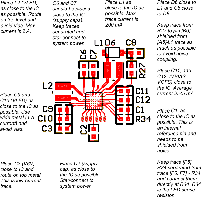
As for all switching power supplies, the layout is an important step in the design, especially at high peak currents and high switching frequencies. If the layout is not carefully done, the regulators could show stability problems as well as EMI problems. Therefore, use wide and short traces for the main current path and for the power ground tracks. Input capacitors, output capacitors, and inductors should be placed as close as possible to the IC.
10.2 Layout Example
 Figure 38. Layout
Table 29. Layout Components
| LABEL | DESCRIPTION |
|---|---|
| C1 | V2V5 output filter cap |
| C2 | VINA input cap |
| C3 | V6V output filter cap |
| C6 | VINL input cap |
| C7 | VINR input cap |
| C8 | VRST output filter cap |
| C9 | VLED output filter cap |
| C10 | VLED output filter cap |
| C11 | VBIAS output filter cap |
| C12 | VOFS output filter cap |
| D6 | VRST rectifying diode |
| L1 | DMD supply inductor |
| L2 | VLED buck-boost inductor |
| R27 | 100k VRST feedback resistor |
| R34 | 100m RLIM sense resistor |