DLPS052A October   2015  – September 2023 DLPA3000

PRODUCTION DATA  

  1.   1
  2. Features
  3. Applications
  4. Description
  5. Revision History
  6. Description (cont.)
  7. Pin Configuration and Functions
  8. Specifications
    1. 7.1 Absolute Maximum Ratings
    2. 7.2 ESD Ratings
    3. 7.3 Recommended Operating Conditions
    4. 7.4 Thermal Information
    5. 7.5 Electrical Characteristics
    6. 7.6 SPI Timing Parameters
  9. Detailed Description
    1. 8.1 Overview
    2. 8.2 Functional Block Diagram
    3. 8.3 Feature Description
      1. 8.3.1 Supply and Monitoring
        1. 8.3.1.1 Supply
        2. 8.3.1.2 Monitoring
          1. 8.3.1.2.1 Block Faults
          2. 8.3.1.2.2 Low Battery and UVLO
          3. 8.3.1.2.3 Auto LED Turn Off Functionality
          4. 8.3.1.2.4 Thermal Protection
      2. 8.3.2 Illumination
        1. 8.3.2.1 Programmable Gain Block
        2. 8.3.2.2 LDO Illum
        3. 8.3.2.3 Illumination Driver A
        4. 8.3.2.4 RGB Strobe Decoder
          1. 8.3.2.4.1 Break Before Make (BBM)
          2. 8.3.2.4.2 Openloop Voltage
          3. 8.3.2.4.3 Transient Current Limit
        5. 8.3.2.5 Illumination Monitoring
          1. 8.3.2.5.1 Power Good
          2. 8.3.2.5.2 Ratio Metric Overvoltage Protection
        6. 8.3.2.6 Load Current and Supply Voltage
        7. 8.3.2.7 Illumination Driver Plus Power FETS Efficiency
      3. 8.3.3 DMD Supplies
        1. 8.3.3.1 LDO DMD
        2. 8.3.3.2 DMD HV Regulator
          1. 8.3.3.2.1 Power-Up and Power-Down Timing
        3. 8.3.3.3 DMD/DLPC Buck Converters
        4. 8.3.3.4 DMD Monitoring
          1. 8.3.3.4.1 Power Good
          2. 8.3.3.4.2 Overvoltage Fault
      4. 8.3.4 Buck Converters
        1. 8.3.4.1 LDO Bucks
        2. 8.3.4.2 General Purpose Buck Converters
        3. 8.3.4.3 Buck Converter Monitoring
          1. 8.3.4.3.1 Power Good
          2. 8.3.4.3.2 Overvoltage Fault
        4. 8.3.4.4 Buck Converter Efficiency
      5. 8.3.5 Auxiliary LDOs
      6. 8.3.6 Measurement System
      7. 8.3.7 Digital Control
        1. 8.3.7.1 SPI
        2. 8.3.7.2 Interrupt
        3. 8.3.7.3 Fast-Shutdown in Case of Fault
    4. 8.4 Device Functional Modes
    5. 8.5 Register Maps
  10. Application and Implementation
    1. 9.1 Application Information
    2. 9.2 Typical Applications
      1. 9.2.1 Typical Application Setup Using DLPA3000
        1. 9.2.1.1 Design Requirements
        2. 9.2.1.2 Detailed Design Procedure
        3. 9.2.1.3 Application Curve
      2. 9.2.2 Typical Application with DLPA3000 Internal Block Diagram
  11. 10Power Supply Recommendations
  12. 11Layout
    1. 11.1 Layout Guidelines
    2. 11.2 Layout Example
    3. 11.3 SPI Connections
    4. 11.4 RLIM Routing
    5. 11.5 LED Connection
    6. 11.6 Thermal Considerations
  13. 12Device and Documentation Support
    1. 12.1 Third-Party Products Disclaimer
    2. 12.2 Device Support
      1. 12.2.1 Device Nomenclature
    3. 12.3 Related Links
    4. 12.4 Receiving Notification of Documentation Updates
    5. 12.5 Support Resources
    6. 12.6 Trademarks
    7. 12.7 Support Resources
    8. 12.8 Electrostatic Discharge Caution
    9. 12.9 Glossary
  14. 13Mechanical, Packaging, and Orderable Information

Package Options

Mechanical Data (Package|Pins)
Thermal pad, mechanical data (Package|Pins)
Orderable Information

Layout Example

Figure 11-2 shows a layout example of a buck converter, illustrating the optimal routing and placement of components around the DLPA3000. Use this as a reference for a general purpose buck2 (PWR6). The layout example illustrates the inductor and its accompanying capacitors are as close as possible to their corresponding pins, using the thickest possible traces. The capacitors use multiple vias to the ground layer to maintain a low resistance path and minimize the distance between the ground connections of the output capacitors and the ground connections of the buck converter.
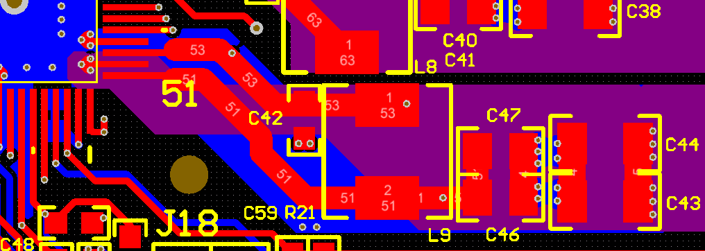
GUID-2DDC028A-0418-4777-854A-72293298DBEA-low.gif Figure 11-2 Practical Layout

A proper layout requires short traces and separate power grounds to avoid losses from trace resistance and to avoid ground shifting. Use high quality capacitors with low ESR to keep capacitor losses minimal and to maintain an acceptable voltage ripple at the output.

Use a RC snubber network to avoid EMI that can occur when switching high currents at high frequencies. The EMI may have a higher amplitude and frequency than the switching voltage.