DLPS052A October   2015  – September 2023 DLPA3000

PRODUCTION DATA  

  1.   1
  2. Features
  3. Applications
  4. Description
  5. Revision History
  6. Description (cont.)
  7. Pin Configuration and Functions
  8. Specifications
    1. 7.1 Absolute Maximum Ratings
    2. 7.2 ESD Ratings
    3. 7.3 Recommended Operating Conditions
    4. 7.4 Thermal Information
    5. 7.5 Electrical Characteristics
    6. 7.6 SPI Timing Parameters
  9. Detailed Description
    1. 8.1 Overview
    2. 8.2 Functional Block Diagram
    3. 8.3 Feature Description
      1. 8.3.1 Supply and Monitoring
        1. 8.3.1.1 Supply
        2. 8.3.1.2 Monitoring
          1. 8.3.1.2.1 Block Faults
          2. 8.3.1.2.2 Low Battery and UVLO
          3. 8.3.1.2.3 Auto LED Turn Off Functionality
          4. 8.3.1.2.4 Thermal Protection
      2. 8.3.2 Illumination
        1. 8.3.2.1 Programmable Gain Block
        2. 8.3.2.2 LDO Illum
        3. 8.3.2.3 Illumination Driver A
        4. 8.3.2.4 RGB Strobe Decoder
          1. 8.3.2.4.1 Break Before Make (BBM)
          2. 8.3.2.4.2 Openloop Voltage
          3. 8.3.2.4.3 Transient Current Limit
        5. 8.3.2.5 Illumination Monitoring
          1. 8.3.2.5.1 Power Good
          2. 8.3.2.5.2 Ratio Metric Overvoltage Protection
        6. 8.3.2.6 Load Current and Supply Voltage
        7. 8.3.2.7 Illumination Driver Plus Power FETS Efficiency
      3. 8.3.3 DMD Supplies
        1. 8.3.3.1 LDO DMD
        2. 8.3.3.2 DMD HV Regulator
          1. 8.3.3.2.1 Power-Up and Power-Down Timing
        3. 8.3.3.3 DMD/DLPC Buck Converters
        4. 8.3.3.4 DMD Monitoring
          1. 8.3.3.4.1 Power Good
          2. 8.3.3.4.2 Overvoltage Fault
      4. 8.3.4 Buck Converters
        1. 8.3.4.1 LDO Bucks
        2. 8.3.4.2 General Purpose Buck Converters
        3. 8.3.4.3 Buck Converter Monitoring
          1. 8.3.4.3.1 Power Good
          2. 8.3.4.3.2 Overvoltage Fault
        4. 8.3.4.4 Buck Converter Efficiency
      5. 8.3.5 Auxiliary LDOs
      6. 8.3.6 Measurement System
      7. 8.3.7 Digital Control
        1. 8.3.7.1 SPI
        2. 8.3.7.2 Interrupt
        3. 8.3.7.3 Fast-Shutdown in Case of Fault
    4. 8.4 Device Functional Modes
    5. 8.5 Register Maps
  10. Application and Implementation
    1. 9.1 Application Information
    2. 9.2 Typical Applications
      1. 9.2.1 Typical Application Setup Using DLPA3000
        1. 9.2.1.1 Design Requirements
        2. 9.2.1.2 Detailed Design Procedure
        3. 9.2.1.3 Application Curve
      2. 9.2.2 Typical Application with DLPA3000 Internal Block Diagram
  11. 10Power Supply Recommendations
  12. 11Layout
    1. 11.1 Layout Guidelines
    2. 11.2 Layout Example
    3. 11.3 SPI Connections
    4. 11.4 RLIM Routing
    5. 11.5 LED Connection
    6. 11.6 Thermal Considerations
  13. 12Device and Documentation Support
    1. 12.1 Third-Party Products Disclaimer
    2. 12.2 Device Support
      1. 12.2.1 Device Nomenclature
    3. 12.3 Related Links
    4. 12.4 Receiving Notification of Documentation Updates
    5. 12.5 Support Resources
    6. 12.6 Trademarks
    7. 12.7 Support Resources
    8. 12.8 Electrostatic Discharge Caution
    9. 12.9 Glossary
  14. 13Mechanical, Packaging, and Orderable Information

Package Options

Mechanical Data (Package|Pins)
Thermal pad, mechanical data (Package|Pins)
Orderable Information

DMD Supplies

This block contains all the supplies needed for the DMD and DLPC (see Figure 8-15). The block comprises:

  • LDO_DMD: for internal supply
  • DMD_HV: regulator generates high voltage supplies
  • Two buck converters: for DLPC/DMD voltages
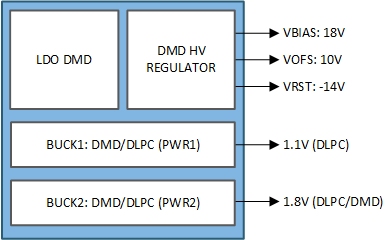
GUID-20230612-SS0I-JXB0-VDPT-XTNHRWRJTCRP-low.gif Figure 8-15 DMD Supplies Blocks

The DMD supplies block is designed to work with the DMD and the related DLPC. The DMD has its own set of supply voltage requirements. Besides the three high voltages, two supplies are needed for the DMD and the related DLPC (DLPC343x-family for instance). These supplies are made by two buck converters.